Supercharge Your Innovation With Domain-Expert AI Agents!

Probe card device

The technology of a probe card and a probe is applied in the field of probe card devices, achieving the effects of convenient realization, simple manufacturing method and saving production cost

Inactive Publication Date: 2010-08-11
SEMICON MFG INT (SHANGHAI) CORP
View PDF1 Cites 1 Cited by
  • Summary
  • Abstract
  • Description
  • Claims
  • Application Information

AI Technical Summary

Problems solved by technology

[0008] The invention provides a probe card device in a chip test system, which is refitted from an adapter board and a general probe card, which solves the problem of the hardware between the originally unmatched probe station and the tester. connection problem

Method used


Image

  • Probe card device
  • Probe card device
  • Probe card device

Examples


Embodiment Construction

[0030] In order to make the above objects, features and advantages of the present invention more comprehensible, specific implementations of the present invention will be described in detail below in conjunction with the accompanying drawings.

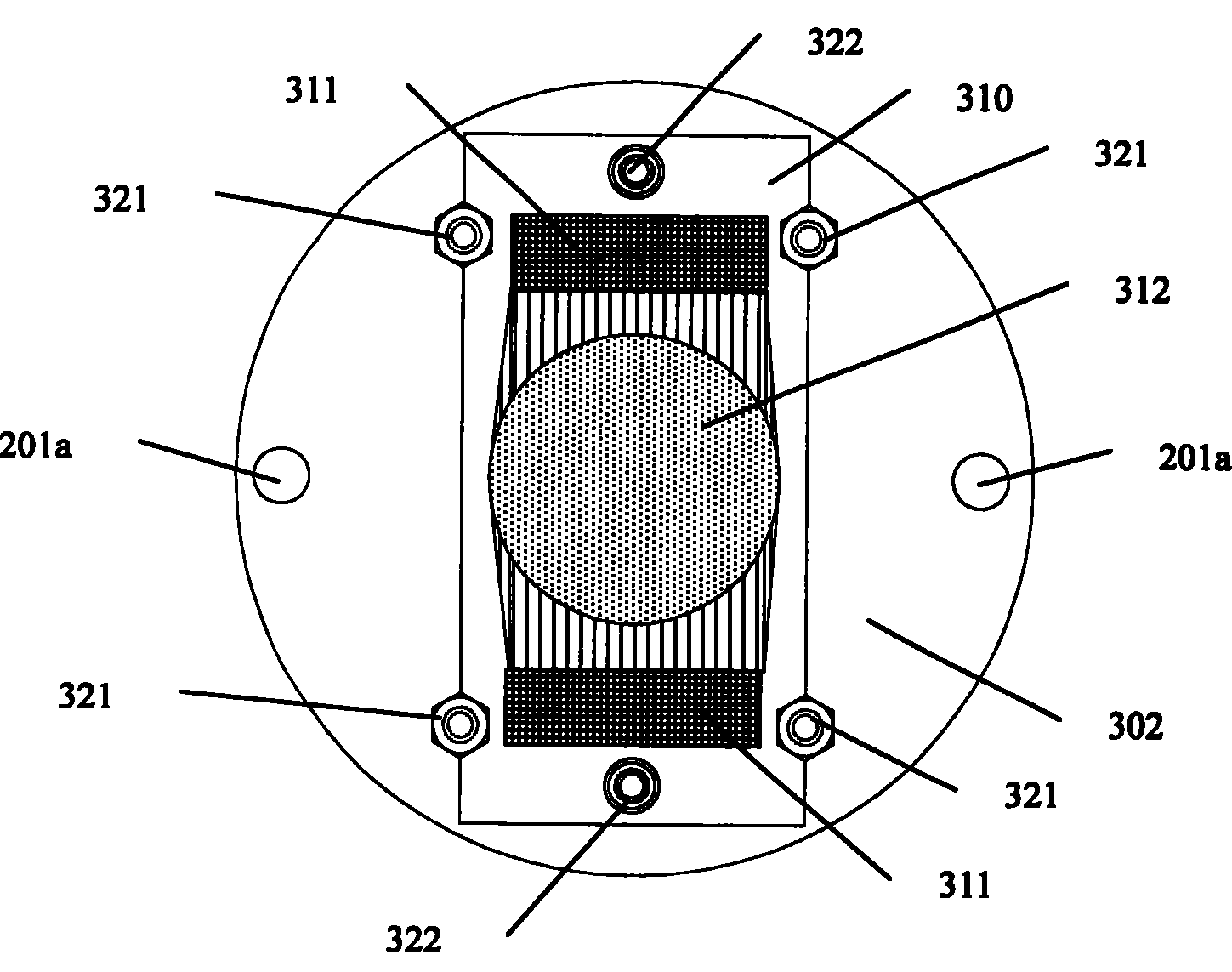
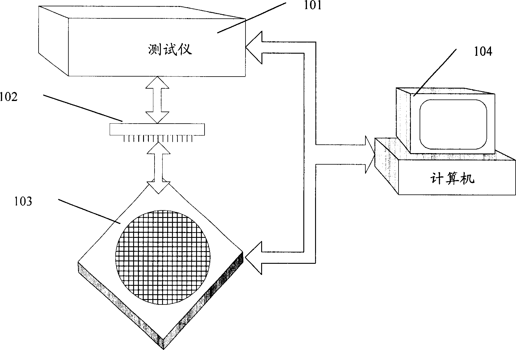
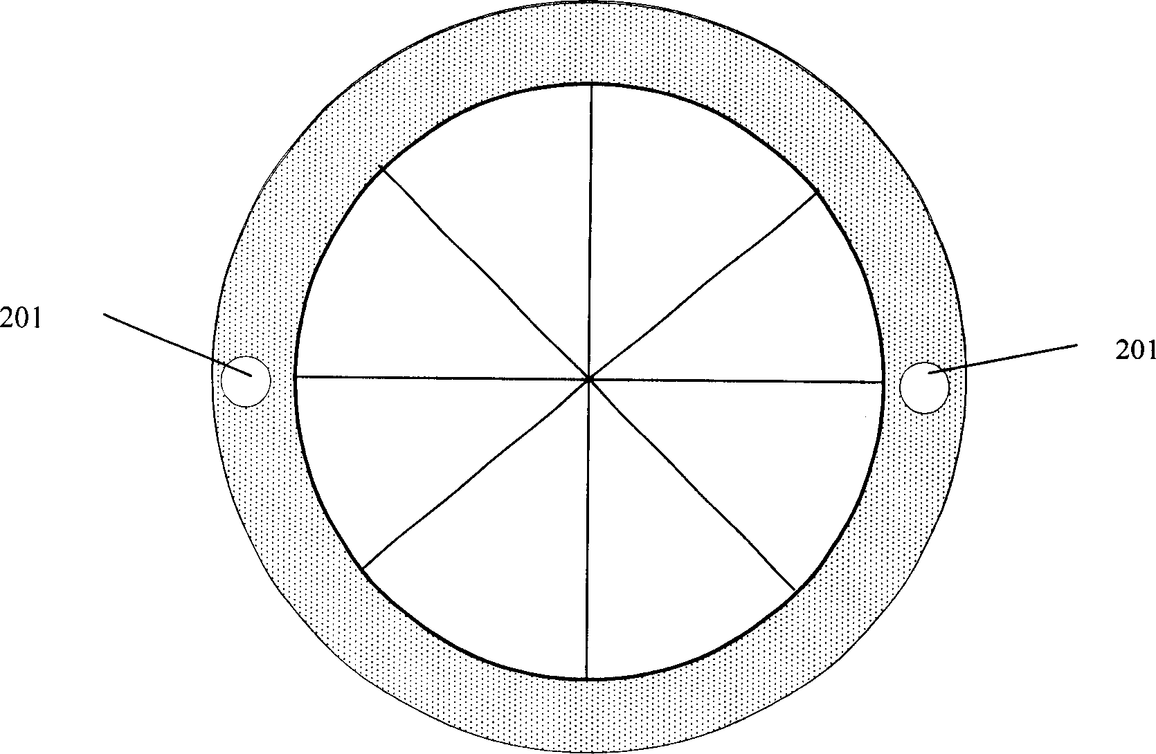
[0031] The first specific embodiment of the probe card device of the chip test system of the present invention is to manufacture and form a probe card device, which can be used for the Maverick test of the automatic probe station TEL-P12 and the original test (FT, Final Test) A connection interface is formed between the instruments to realize a new chip testing function. Figure 2 is a schematic diagram of a dedicated probe card matched with the probe station TEL-P12. As shown in Figure 2, the automatic probe station TEL-P12 was originally matched with the press-fit Agilent4072 parameter tester to form a set of chip parameter test system, so the special probe card assembled on it is also press-fit, and the Maverick tester There is no p...


PUM


Abstract

The utility model discloses a probe card device in chip test system; the probe card device consists of a transfer board and a general probe card, which not only meets the installation requirement of a probe platform to the probe card but also meets the connecting requirement of a test instrument to the probe card; the user doesn't need to buy the new chip test system, doesn't need to replace the hardware including the test instrument and the probe platform and can realize the new test function by replacing the new probe card device and using the original equipment, which effectively saves cost; the utility model has the advantages of convenient installation and wide universality.

Description

technical field [0001] The invention relates to the field of chip testing in the semiconductor manufacturing process, in particular to a probe card device of a chip testing system. Background technique [0002] Due to the rapid introduction of increasingly complex integrated circuits, materials and processes, it is almost impossible in today's silicon wafer manufacturing that every chip meet the specification requirements. In order to correct the problems in the production process and ensure that defective chips are not sent In the hands of customers, chip testing (CP, Circuit Probing) is introduced in the integrated circuit manufacturing process. Chip testing is an electrical parameter measurement and functional test performed on a silicon-level integrated circuit in order to verify the consistency of specifications. The test can verify whether each chip has acceptable electrical performance and complete functions. Electrical specifications vary depending on the purpose of...

Claims


Application Information

Patent Timeline
Patent Type & Authority Patents(China)
IPC IPC(8): G01R1/02G01R1/067G01R1/073G01R31/00H01L21/66
Inventor 刘云海简维廷张荣哲
Owner SEMICON MFG INT (SHANGHAI) CORP
Features
  • R&D
  • Intellectual Property
  • Life Sciences
  • Materials
  • Tech Scout
  • Unparalleled Data Quality
  • Higher Quality Content
  • 60% Fewer Hallucinations
Learn More