Eureka AIR delivers breakthrough ideas for toughest innovation challenges, trusted by R&D personnel around the world.

Method for measuring thin layers in solid state devices

A solid-state, object-based technology, applied in semiconductor/solid-state device testing/measurement, measuring devices, instruments, etc., can solve problems such as unsatisfactory technology and indistinguishable signals

Inactive Publication Date: 2008-01-23
INT BUSINESS MASCH CORP
View PDF0 Cites 12 Cited by
  • Summary
  • Abstract
  • Description
  • Claims
  • Application Information

AI Technical Summary

Problems solved by technology

Recently, fast Fourier transform (FFT) methods have been employed to measure thin layer thickness, however, these methods have not been successfully and reliably applied to thin bonded layers
By thin layers we mean that the reflected acoustic signals returning from the layer are usually combined into a single echo for which thickness measurement is very imprecise or impossible by conventional techniques, due to the The reflections from the top and bottom of the pad overlap each other such that the signal reflected from the top of the bond layer is indistinguishable from the signal reflected from the bottom of the bond layer
[0006] As newer technologies, smaller semiconductor devices require bonding layers thinner than a threshold thickness, where top and bottom echoes start to separate, existing techniques are not satisfactory, and the field has sought to provide support for such thin bonding Measurement technique for accurate non-destructive measurement of layers

Method used


Image

  • Method for measuring thin layers in solid state devices
  • Method for measuring thin layers in solid state devices
  • Method for measuring thin layers in solid state devices

Examples


Embodiment Construction

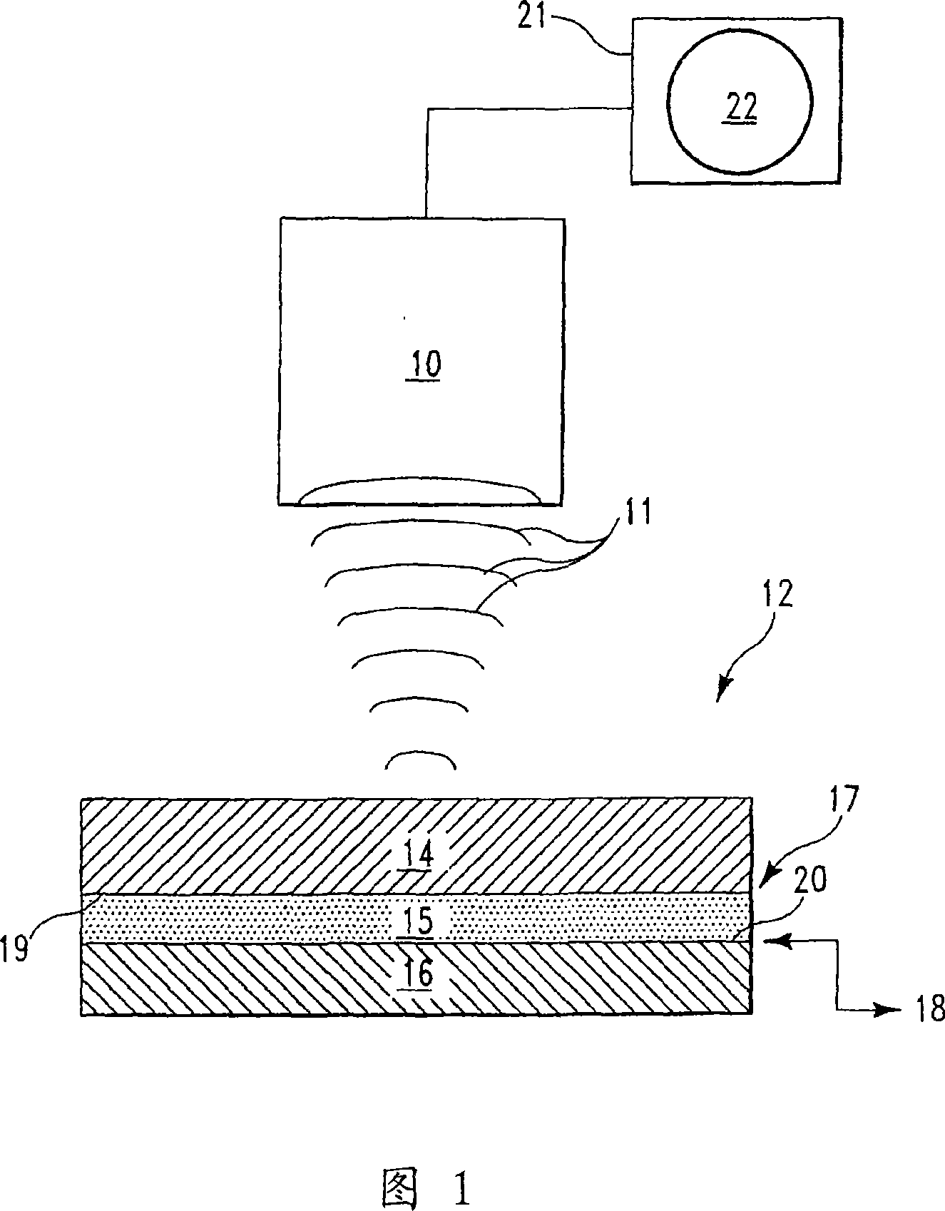
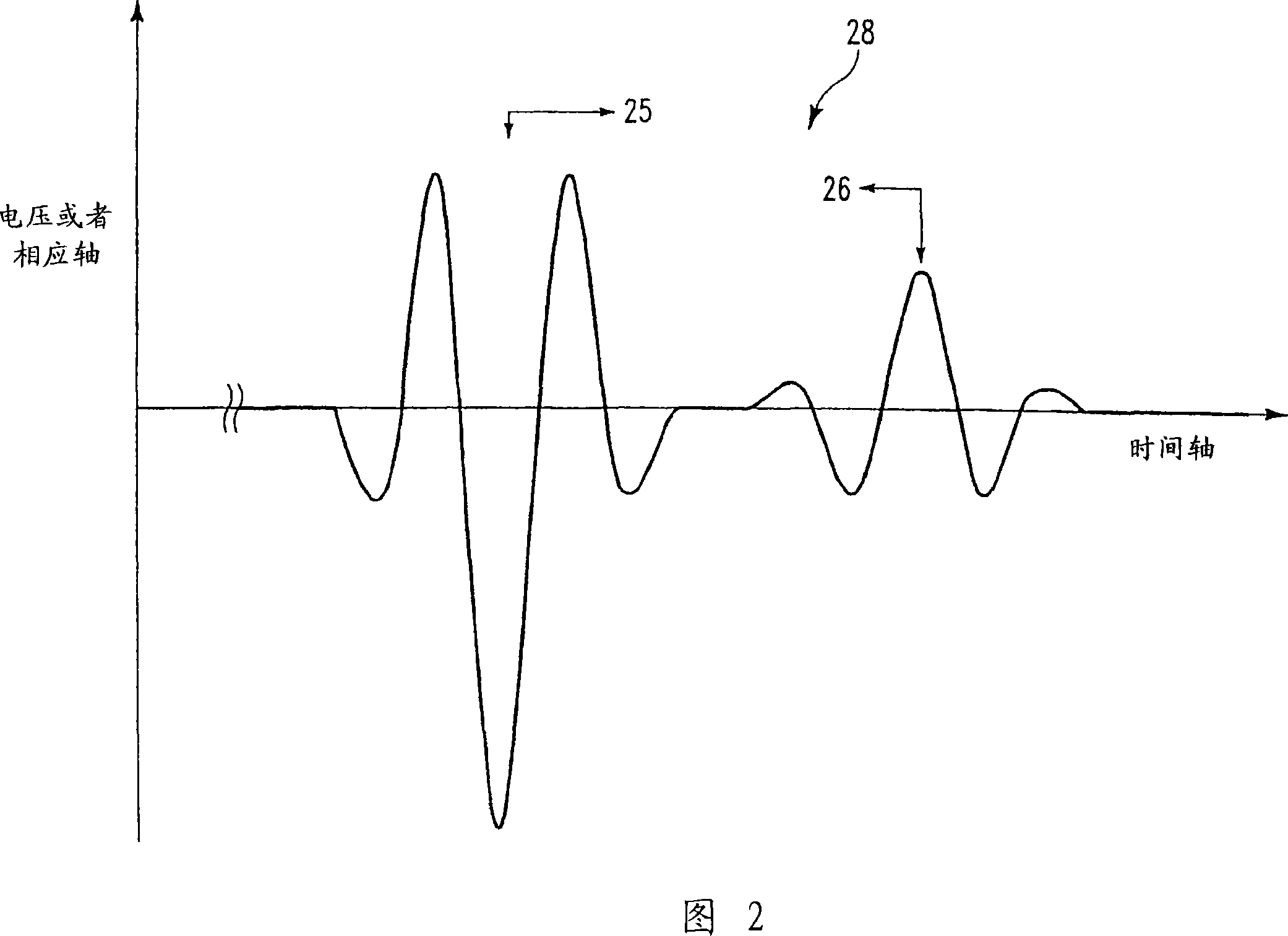
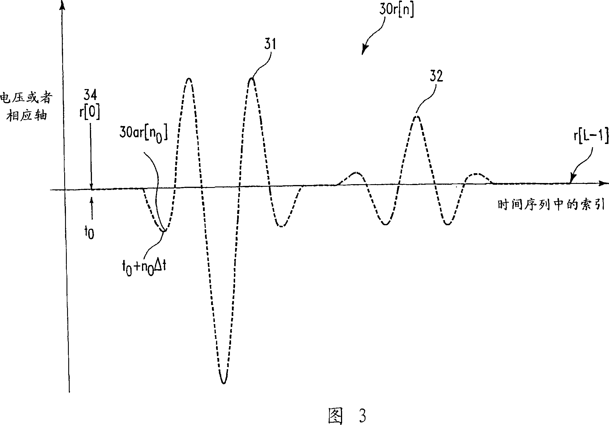
[0022] A full understanding of the features and advantages of the present invention may be better obtained by referring to the accompanying drawings, in particular: Figure 1 schematically illustrates an acoustic microscope, applying sound waves to the surface of an object comprising The middle bond layer is fixed to the first material on the second material; Figure 2 shows when a wave from the microscope of Figure 1 is applied to a device with a bond layer thick enough to produce sufficiently separated primary and secondary echoes The resulting primary and secondary echoes; Figure 3 shows the primary and secondary echoes shown in Figure 2 after these echoes have been digitized into corresponding time series; Figure 4 shows the time Figure 5 shows the primary and secondary echoes returned from the object of Figure 1 when the object contains a bonding layer whose thickness is so thin that the primary and secondary echoes overlap each other; Fig. 6 shows the primary and secondary...


PUM


Abstract

A method of measuring the thickness of a bonding layer using an acoustic signal. The method is accomplished by applying sound waves to the layered object that cause primary and secondary echoes to be reflected from different interfaces; detecting and digitizing the echoes to produce a digital time series that is processed to remove noise; using filtering the time series with a filter matched to the main echo; locating the time position and magnitude of the maximum value of the filtered time series; time shifting and scaling the main echo using the obtained time position and magnitude; subtracting the primary echo transform model to obtain a cleaned time series; filtering the cleaned time series using a filter matched to the secondary echoes; locating the time position of the maximum value of the secondary echo filtered time series; from The transit time is determined from the difference between the time locations of the primary and secondary echoes; and the bond bond thickness is determined, which is equal to half the measured transit time multiplied by the velocity of the sound wave or pulse in the bond bond.

Description

technical field [0001] The present invention relates generally to reflective acoustic microscopy methods for measuring the thickness of bonding layers in bodies, particularly for bonding components together in solid state or microelectronic devices. Background technique [0002] The complexity and compactness of today's electronic devices requires the inclusion of thin bonding layers in various circuit configurations of semiconductor devices, such as may be used to secure semiconductor devices to heat sinks or heat sinks or caps. Measuring the thickness of this bonding layer is very important to ensure that the devices are not only functioning properly but also functioning within their design parameters, especially with respect to device thermal conduction requirements. [0003] Several methods exist for measuring the thickness of such bonding layers. Early but destructive and time-consuming methods required cross-sectioning the device for the thickness of the buried layer ...

Claims


Application Information

Patent Timeline
Patent Type & Authority Applications(China)
IPC IPC(8): G01B17/02H01L21/66
CPCG01B17/02
Inventor 亚历山大·布兰德卡尔·萨瓦德朱利恩·西尔维斯特
Owner INT BUSINESS MASCH CORP
Why Eureka
Eureka Blog
Learn More