[0006]To address these needs,
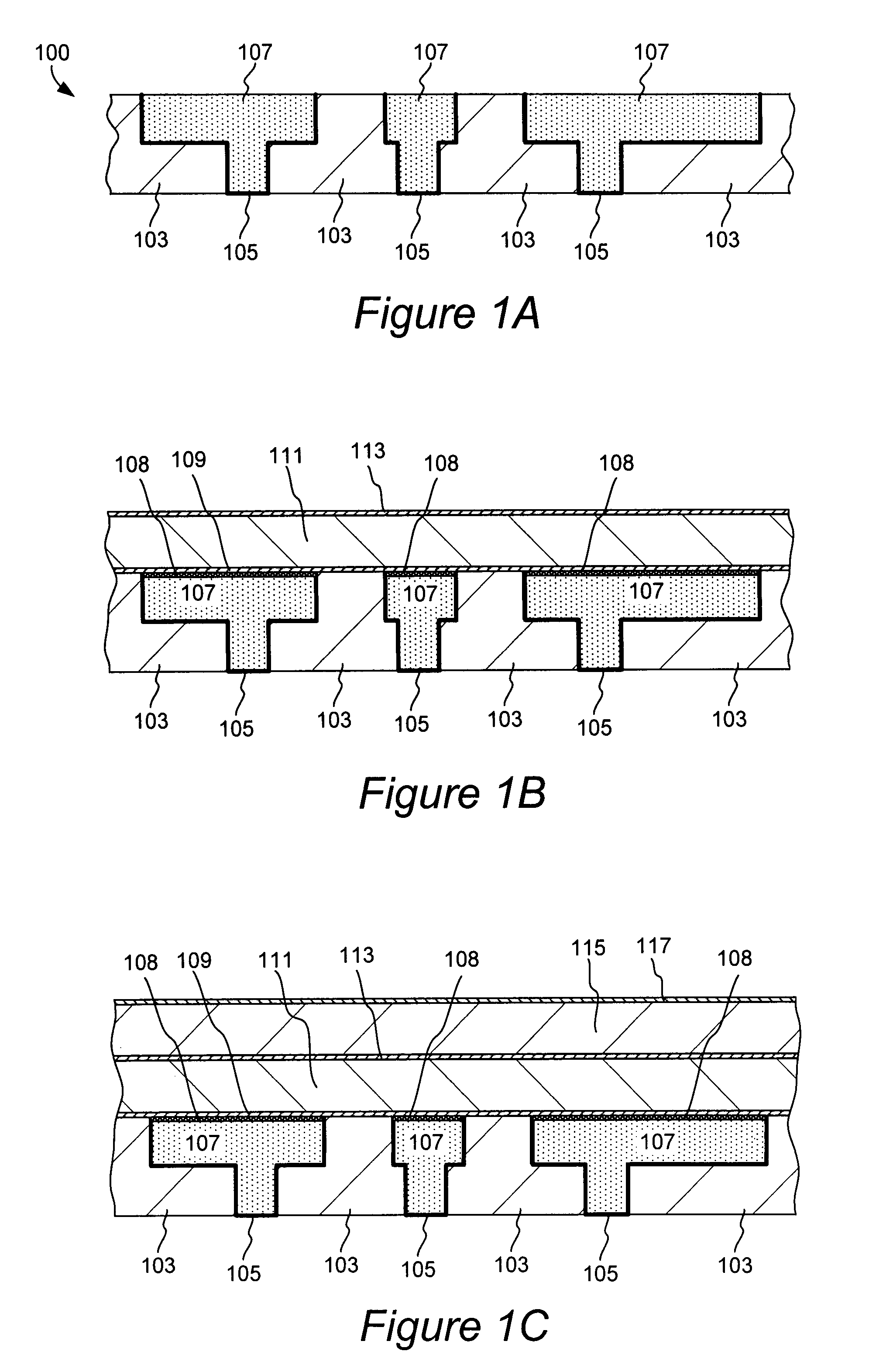
IC devices having interconnects with protective self aligned buffer (PSAB) layers are provided. Methods of forming PSAB layers during IC device fabrication are also described herein. PSAB layers are layers of material that are selectively formed at the surface of metal layers of a partially fabricated
semiconductor device. PSAB layers may be capable of improving several properties of Damascene interconnects. For example, a PSAB layer may promote improved adhesion between a metal layer and an adjacent dielectric
diffusion barrier layer. Further, PSAB layers can protect metal surfaces from inadvertent oxidation during fabrication processes and can lead to a decrease in metal
electromigration during end use of a
semiconductor device. Methods of forming PSAB-containing interconnects having reduced
stress migration parameters are also provided.
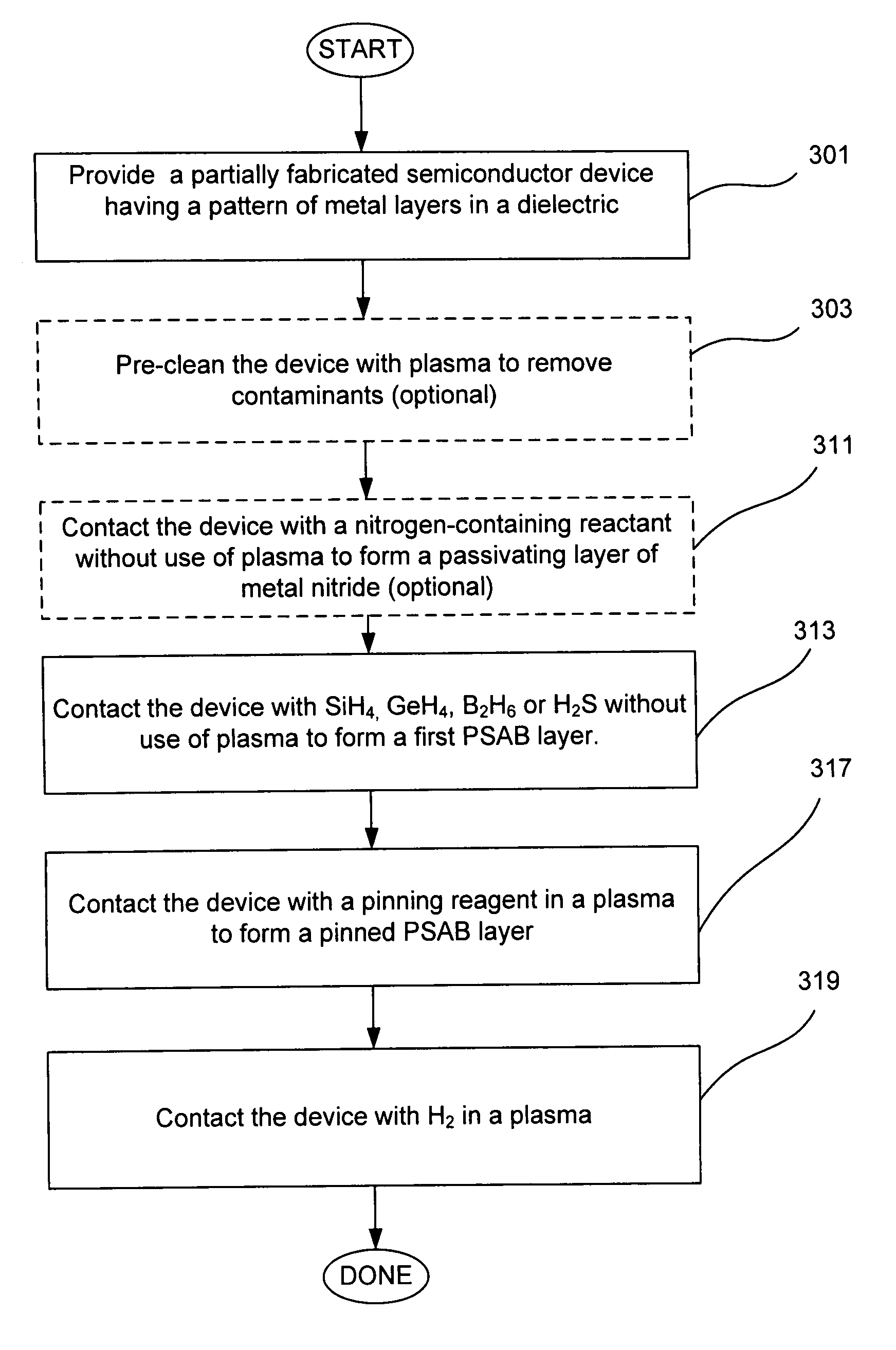
[0007]In some embodiments, a PSAB layer is formed entirely within the top portion of a metal layer, such that it is substantially at the same level as the plane of a dielectric field region adjacent to the metal layer. This can be accomplished by chemically transforming exposed metal atoms to a desired material. For example, Cu can react with SiH4 to form a thin PSAB layer of CuxSiy within the top portion of metal layer. While PSAB layers generally increase resistance of interconnects, such resistance shift can be efficiently controlled. Specifically, thickness of PSAB layers, and, consequently, resistance of an interconnect can be controlled by partially passivating exposed metal surfaces, prior to formation of the PSAB layer. Such
passivation can be accomplished by, for example, controllably reacting surface atoms with a
nitrogen-containing compound (e.g., NH3) to form a metal
nitride. Such
passivation depletes the amount of metal atoms (in a zero
oxidation state) that are available for reaction to form the PSAB layer, and, consequently, controls the thickness of the PSAB layer and resistance of an interconnect.
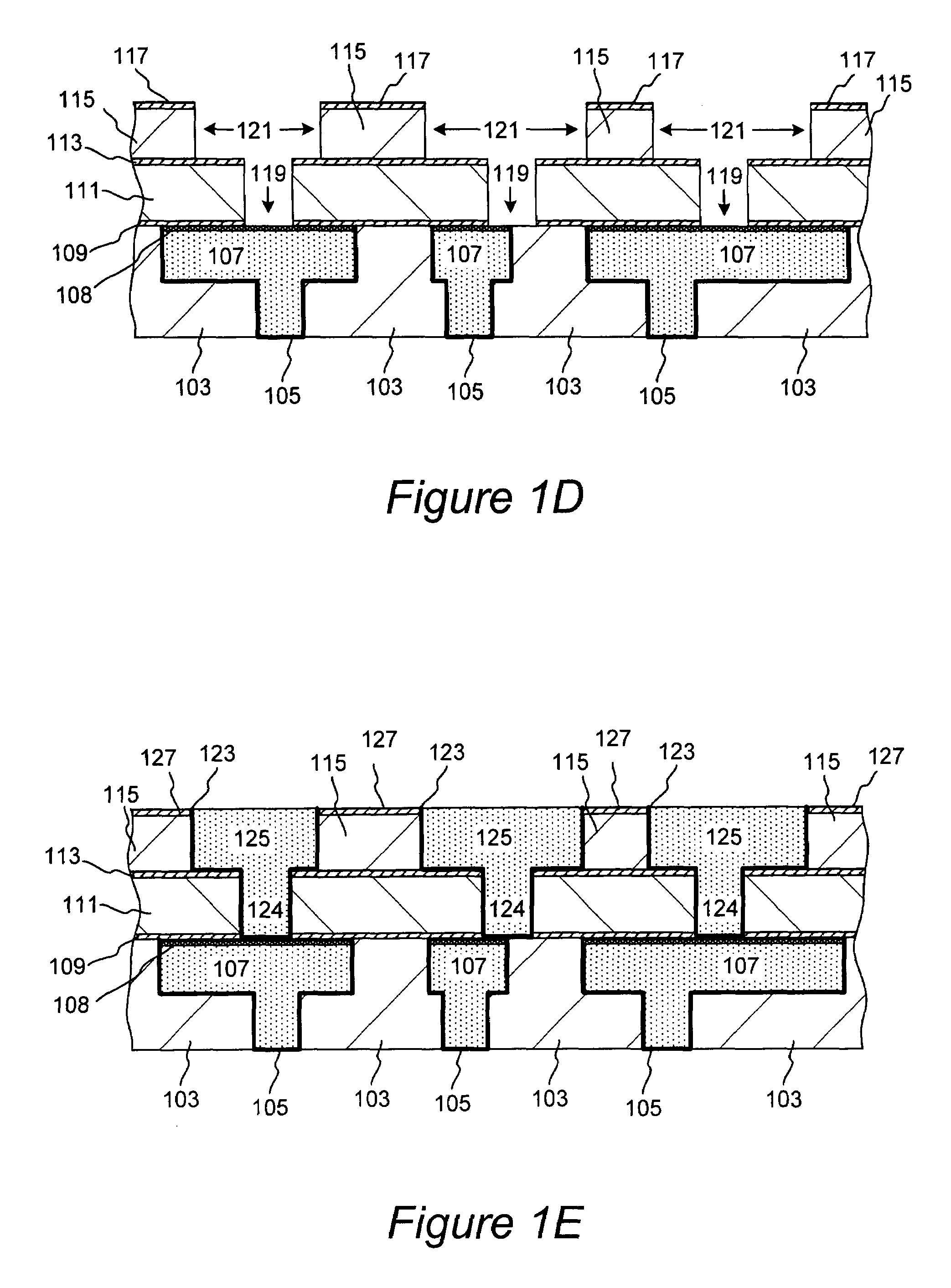
[0011]In some embodiments, the first PSAB layer resides entirely within the metal layer. The depth of the first PSAB layer is regulated by an amount of the passivated material (e.g., metal
nitride) formed in the first operation, and can range, for example, between 10-1000 Å. The greater the amount of the passivated material formed at the metal surface, the less is the depth of the first PSAB layer. Thus, the thickness of the first PSAB layer, and, consequently, resistance of interconnect, is controlled via a partial passivation of exposed metal surface. In certain embodiments, PSAB layers having a thickness
ranging between about 10-60 Å can be formed in a controlled fashion. Control can be achieved, in some embodiments, by regulating the
contact time of the
nitrogen containing passivating
reagent with the substrate.
[0017]In some embodiments, the first formed PSAB layer may be further treated to form a so-called “pinned” PSAB layer. “Pinning” is often used to chemically transform intermediates and by-products generated during formation of the first PSAB layer to materials that do not readily diffuse into the depth of metal lines. Thus, pinning, controls interconnect resistance by limiting diffusion of non-conducting species into metal-filled vias and trenches. In some embodiments, pinning can also partially or completely chemically transform the material of the first PSAB layer. Certain pinning reagents, such as hydrocarbons, form pinned PSAB layers that result in improved
stress migration performance of formed interconnects.
[0023]In another aspect, a method of forming a PSAB layer of material includes contacting the partially fabricated
semiconductor device with a PSAB forming reactant to form a first PSAB layer, followed by a pinning operation, which comprises contacting the first PSAB layer with a pinning process gas in a
plasma and contacting the device with H2 in a
plasma. H2
plasma treatment can be performed concurrently with the pinning operation or subsequent to pinning, as a post-treatment step. Use of H2
plasma treatment as a pinning reactant reduces
stress migration in the formed interconnects.
[0024]In another aspect a method of forming a PSAB layer of material includes contacting the partially fabricated
semiconductor device with a PSAB forming reactant to form a first PSAB layer, followed by a pinning operation, which comprises contacting the first PSAB layer with a process gas comprising a
hydrocarbon to form a pinned PSAB layer. Use of
hydrocarbon as a pinning reactant reduces stress migration in the formed interconnects.

