Protective self-aligned buffer layers for damascene interconnects

a buffer layer and damascene technology, applied in the direction of thin material handling, electrical equipment, transportation and packaging, etc., can solve the problem of the dimensions of ic device features, and achieve the effect of high mobility

Active Publication Date: 2009-08-18
NOVELLUS SYSTEMS
View PDF20 Cites 57 Cited by
  • Summary
  • Abstract
  • Description
  • Claims
  • Application Information

AI Technical Summary

Benefits of technology

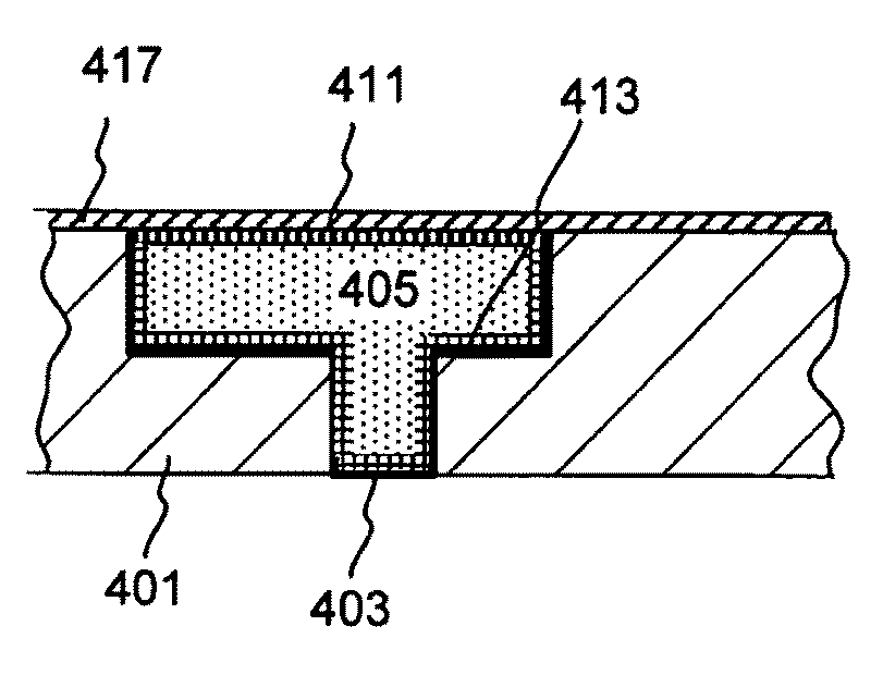
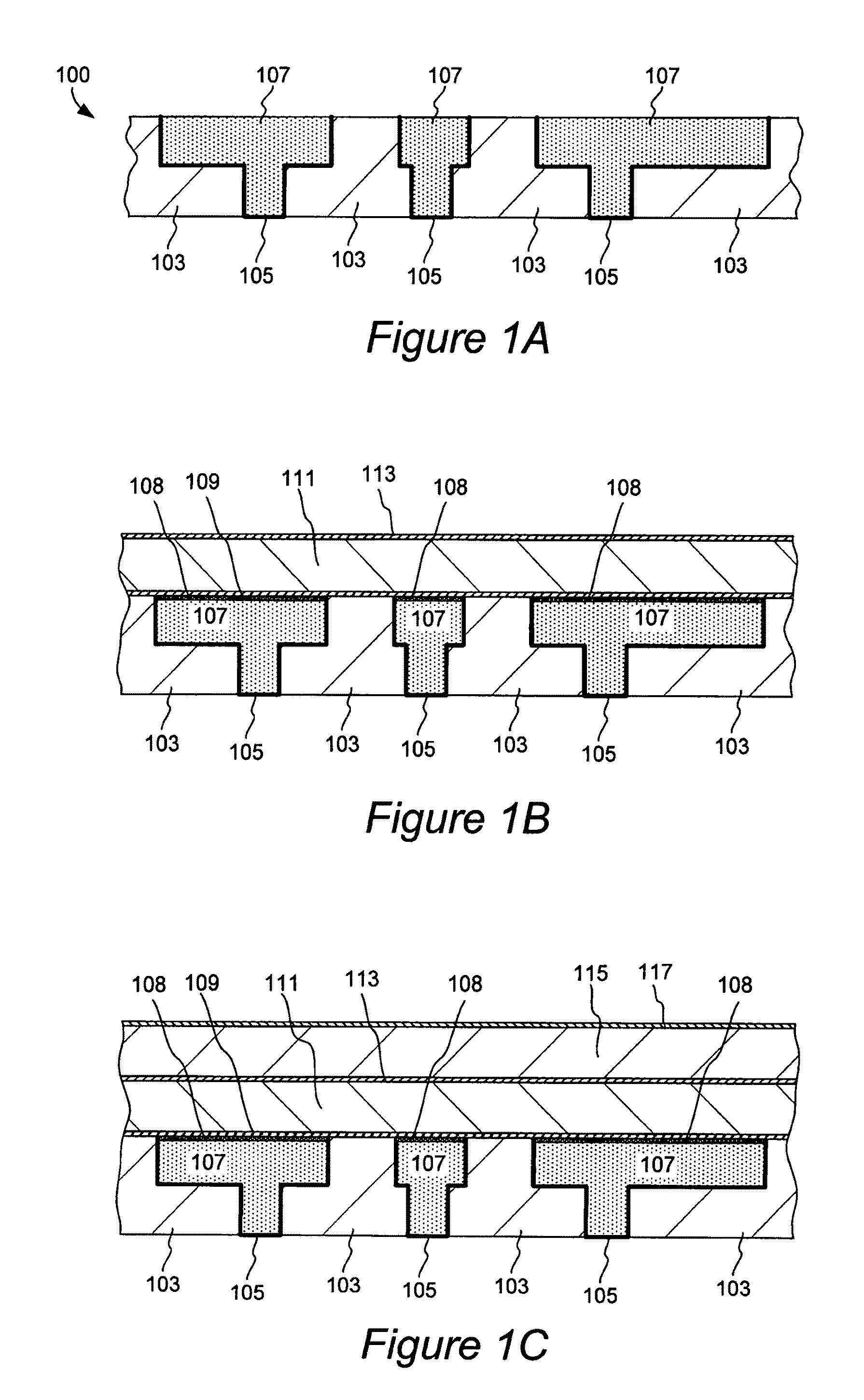
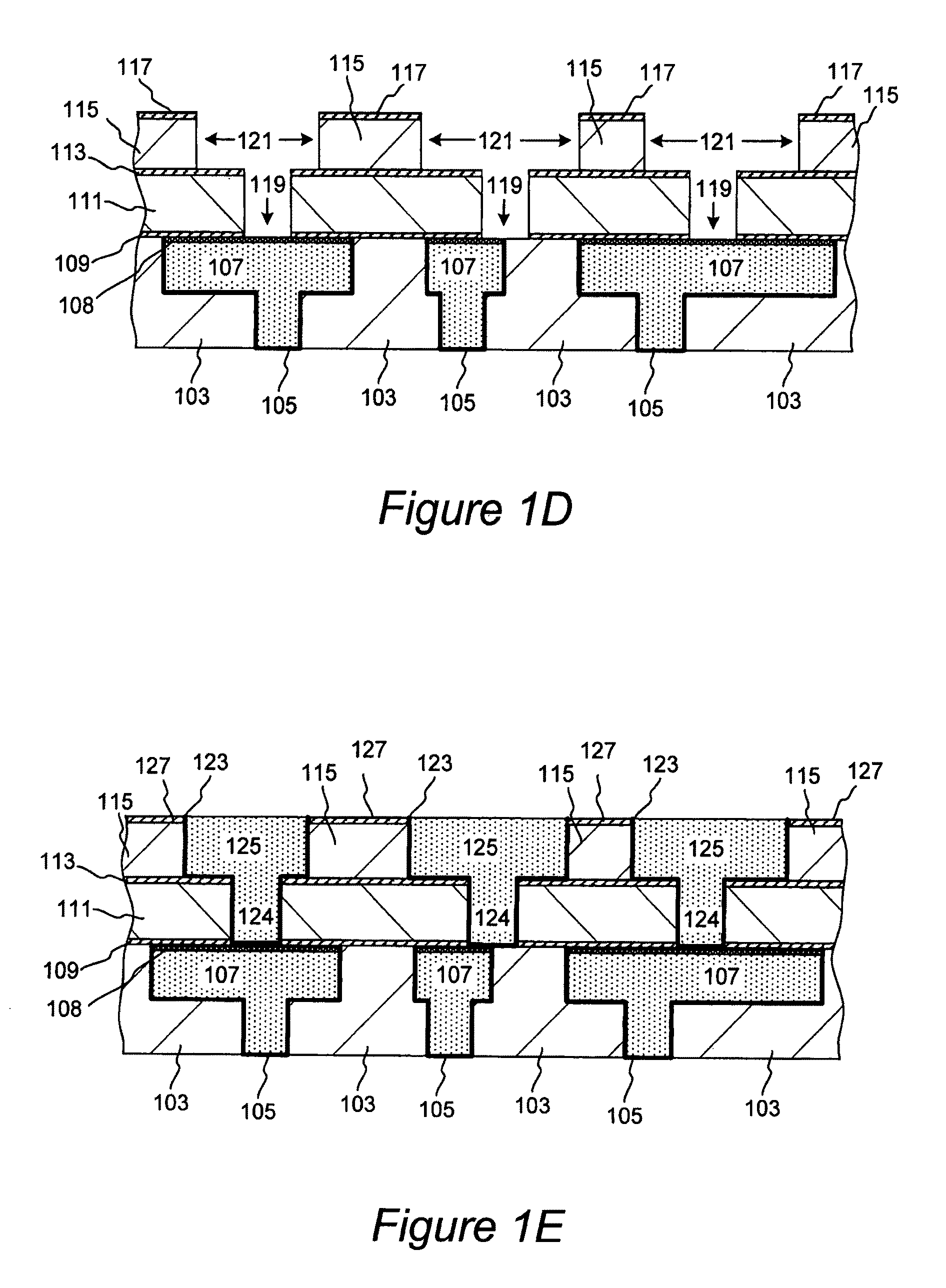
[0006]To address these needs, IC devices having interconnects with protective self aligned buffer (PSAB) layers are provided. Methods of forming capping and encapsulating PSAB layers during IC device fabrication are also described herein. Capping PSAB layers are layers of material that are selectively formed at the surface of metal layers of a partially fabricated semiconductor device. Encapsulating PSAB layers are layers of material that are formed such that the metal layer is encapsulated by the PSAB material, e.g., the PSAB layer lines the top, bottom, and side portions of metal-filled vias and trenches and resides at the interfaces between the metal and the surrounding diffusion barrier layers. Advantageously, provided methods allow formation of encapsulating PSAB layers by treating the metal-filled recesses, rather than by pre-depositing a lining material before the metal fill is formed. These methods make use of high mobility of certain PSAB materials within the metal-filled Damascene interconnects.

Problems solved by technology

Fabrication of these interconnects presents several challenges, which become more and more significant as the dimensions of IC device features continue to shrink.

Method used


Image

  • Protective self-aligned buffer layers for damascene interconnects
  • Protective self-aligned buffer layers for damascene interconnects
  • Protective self-aligned buffer layers for damascene interconnects

Examples


examples

[0127]One example of a device, containing an encapsulating PSAB layer is illustrated in FIG. 8. FIG. 8 provides a Secondary Ion Mass Spectroscopy (SIMS) plot of an interconnect prepared according to a method described herein. The SIMS plot presents concentrations of various components in the device as a function of their position within an interconnect. Position at a zero angstrom depth corresponds to the surface of the dielectric diffusion barrier layer. Curves (a), (b), (c), (d), (e) and (f), present concentrations of Si, Ta, Ge, O, Cu, and N respectively. It can be seen that curve (c) corresponding to germanium concentration has two peaks corresponding to two portions of an encapsulating PSAB layer within the interconnect. One peak at the depth of about 190 Å corresponds to the “top” portion of an encapsulating PSAB layer at the interface between copper layer and the dielectric diffusion barrier, while the second peak at the depth of about 950 Å corresponds to the “bottom” portio...

example 2

[0137]The 300 mm wafer was pre-heated at the first station at 275° C. and 2.3 torr for 60 seconds. N2 was flowed into the chamber at a flow rate of 5000 sccm during pre-heating.

[0138]Then, the substrate was plasma pre-cleaned at the same station. H2 was flowed at a flow rate of 4000 sccm; HF RF plasma power of 740-870 W was used (no LF power was applied). Pre-cleaning was performed at 4.2 torr and 275° C. for 15 seconds.

[0139]After pre-cleaning the substrate was treated with SiH4 without use of plasma at the same station. SiH4 was introduced at 120 sccm flow rate concurrently with NH3 introduced at a flow rate of 4000 sccm. SiH4 treatment was performed at 2.3 torr and 275° C. for 2 seconds.

[0140]Then the substrate was treated with GeH4 at the same station. During GeH4 treatment, GeH4 was introduced at a flow rate of 50 sccm, H2 at 9000 sccm and N2 at 18000 sccm. GeH4 treatment was performed at 1.5 torr and 275° C. for 2 seconds.

[0141]The substrate was then subjected to a pinning ope...

example 3

[0143]The 300 mm wafer was pre-heated at the first station at 275° C. and 2.3 torr for 60 seconds. N2 was flowed into the chamber at a flow rate of 5000 sccm during pre-heating.

[0144]Then, the substrate was plasma pre-cleaned at the same station. H2 was flowed at a flow rate of 4000 sccm; HF RF plasma power of 740-870 W was used (no LF power was applied). Pre-cleaning was performed at 4.2 torr and 275° C. for 15 seconds.

[0145]After pre-cleaning the substrate was treated with SiH4 without use of plasma at the same station. SiH4 was introduced at 120 sccm flow rate concurrently with H2 introduced at a flow rate of 4000 sccm. SiH4 treatment was performed at 2.3 torr and 275° C. for 4 seconds.

[0146]Then the substrate was treated with GeH4 at the same station. During GeH4 treatment, GeH4 was introduced at a flow rate of 50 sccm, and H2 at 9000 sccm. GeH4 treatment was performed at 1.5 torr and 275° C. for 2 seconds.

[0147]The substrate was then subjected to a pinning operation. Pinning wa...


PUM

PropertyMeasurementUnit
pressureaaaaaaaaaa
temperatureaaaaaaaaaa
dielectric constantaaaaaaaaaa

Abstract

Capping protective self aligned buffer (PSAB) layers are layers of material that are selectively formed at the surface of metal layers in a partially fabricated semiconductor device. Encapsulating PSAB layers are formed not only at the surface of the metal layers, but also within the unexposed portions of the metal lines. Encapsulating PSAB layer, for example, can surround the metal line with the PSAB material, thereby protecting interfaces between the metal line and diffusion barriers. Encapsulating PSAB layers can be formed by treating the exposed surfaces of metal lines with GeH4. Capping PSAB layers can be formed by treating the exposed surfaces of metal lines with SiH4. Interconnects having both a silicon-containing capping PSAB layer and a germanium-containing encapsulating PSAB layer provide good performance in terms of adhesion, resistance shift, and electromigration characteristics.

Description

CROSS-REFERENCE TO RELATED APPLICATIONS[0001]This application is a continuation claiming priority from U.S. patent application Ser. No. 11 / 726,363, titled “Protective Self-aligned Buffer Layers for Damascene Interconnects” filed Mar. 20, 2007, naming Yu et al. as inventors, which is a continuation-in-part claiming priority from U.S. patent application Ser. No. 11 / 709,293, titled “Protective Self-aligned Buffer Layers for Damascene Interconnects” filed Feb. 20, 2007, naming Chattopadhyay et al. as inventors, which is a continuation-in-part claiming priority from U.S. patent application Ser. No. 10 / 980,076 filed Nov. 3, 2004, now U.S. Pat. No. 7,396,759 titled “Protection of Cu Damascene Interconnects by Formation of a Self-aligned Buffer Layer,” naming van Schravendijk et al. as inventors, which are incorporated herein by reference in their entirety and for all purposes.FIELD OF THE INVENTION[0002]The present invention pertains to methods of forming layers of material on a partially ...

Claims


Application Information

Patent Timeline
Patent Type & Authority Patents(United States)
IPC IPC(8): H01L21/44
CPCH01L21/67207H01L21/76834H01L21/76846H01L21/76886H01L21/76856H01L21/76867H01L21/76883H01L21/76849Y10S414/139
Inventor YU, YONGSIKSRIRAM, MANDYAMSHAVIV, ROEYCHATTOPADHYAY, KAUSHIKWU, HUI-JUNG
Owner NOVELLUS SYSTEMS
Why Eureka
Try Eureka