Lithographic apparatus, aberration correction device and device manufacturing method

A technology of aberration correction and lithography equipment, which is applied in the direction of microlithography exposure equipment, photomechanical equipment, photolithography exposure equipment, etc., and can solve problems such as deformation and component heating

Active Publication Date: 2008-01-23
ASML NETHERLANDS BV
View PDF1 Cites 16 Cited by
  • Summary
  • Abstract
  • Description
  • Claims
  • Application Information

AI Technical Summary

Problems solved by technology

Therefore, although the elements of the projection system that project the desired pattern onto the substrate have a very high transmittance, the amount of radiation absorbed by them is not negligible and leads to significant heating of the elements, even when using a projection system for High efficiency temperature control system
Because this heating is non-uniform, this results in distortions in the shape of the element sufficient to cause significant distortion of the projected image

Method used


Image

  • Lithographic apparatus, aberration correction device and device manufacturing method
  • Lithographic apparatus, aberration correction device and device manufacturing method
  • Lithographic apparatus, aberration correction device and device manufacturing method

Examples


Embodiment Construction

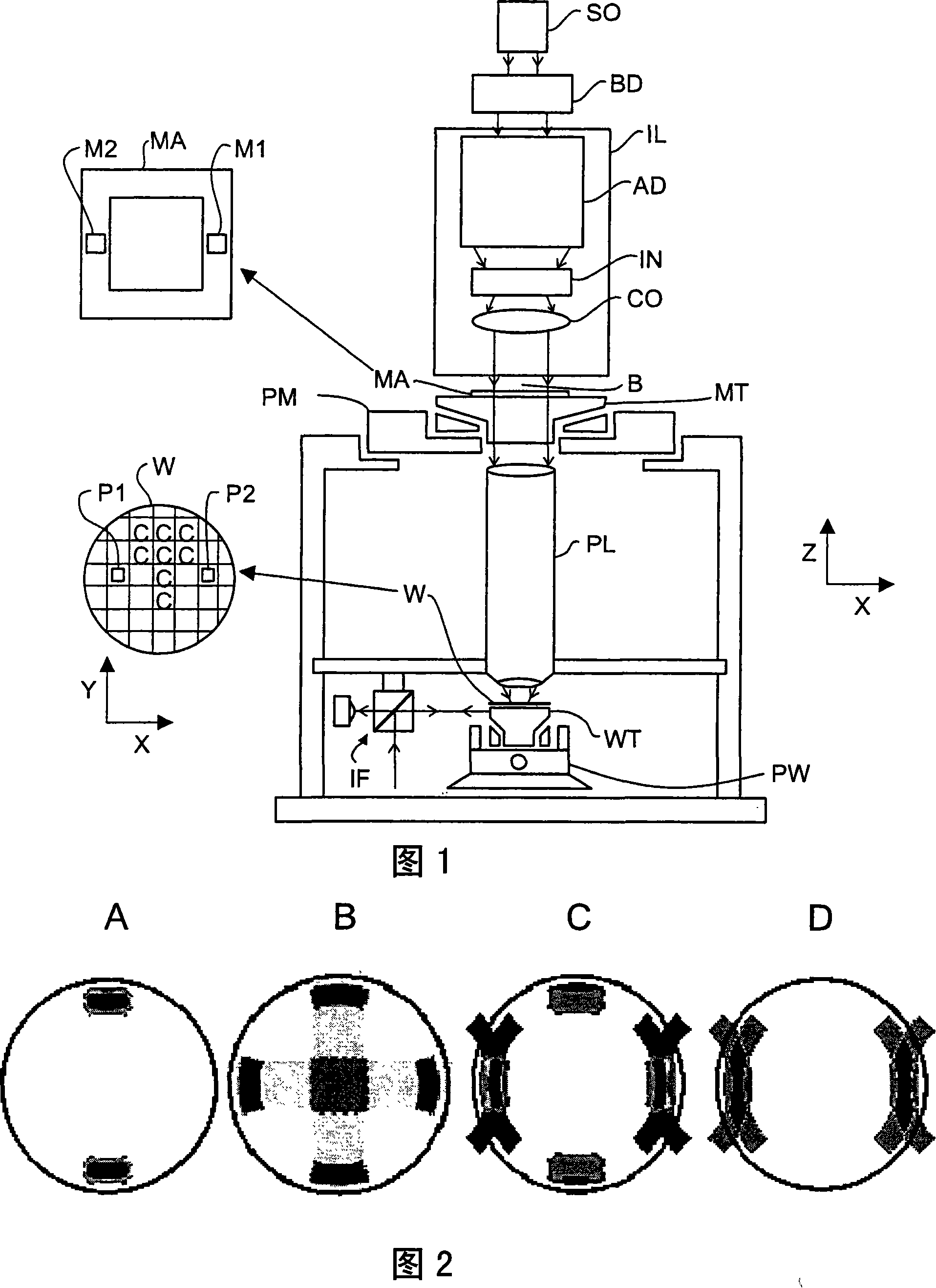
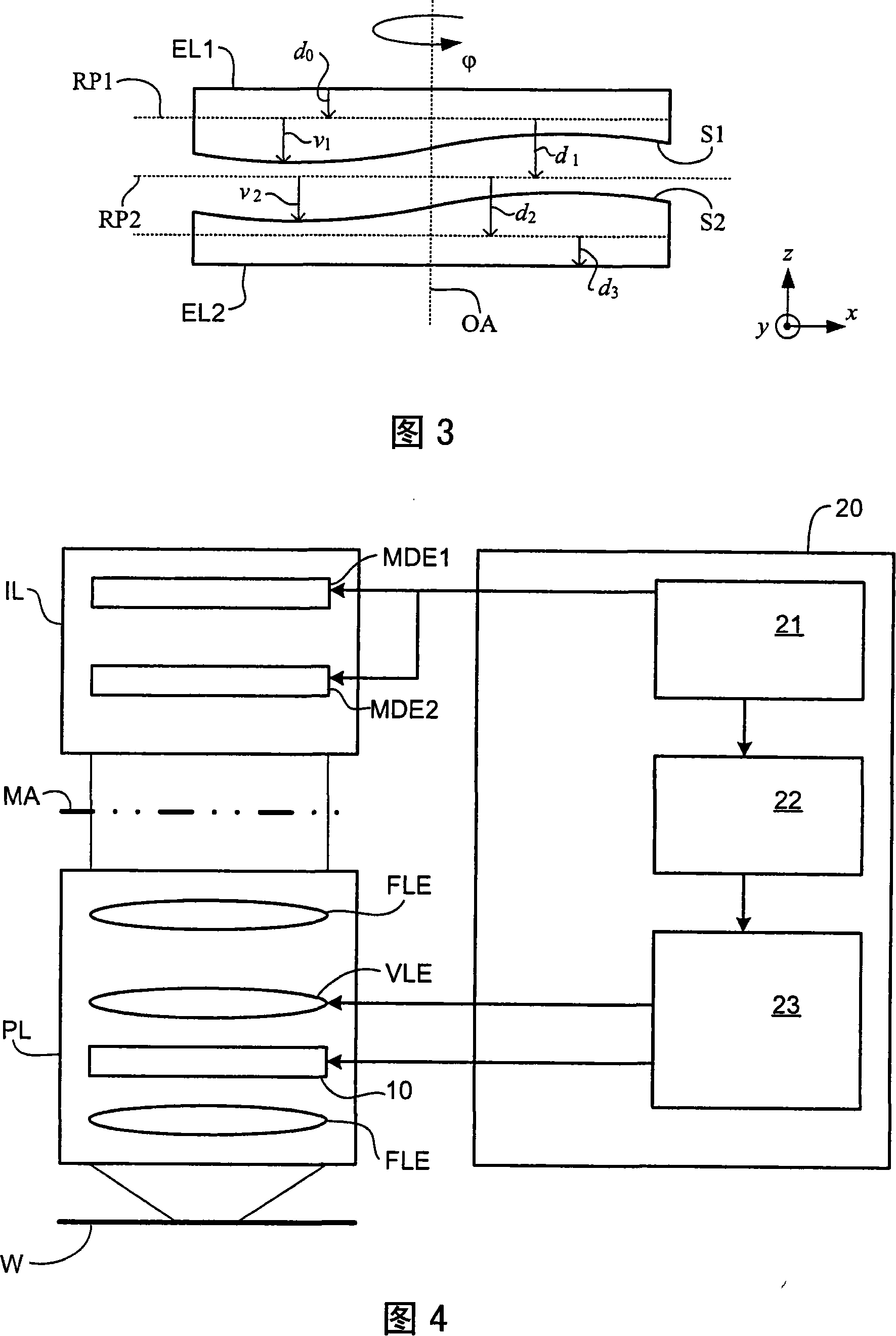
[0043] Fig. 1 schematically shows a lithographic apparatus according to an embodiment of the present invention. The equipment includes:

[0044] An illumination system (illuminator) IL configured for conditioning a radiation beam B (eg UV radiation or DUV radiation).

[0045] a support structure (e.g. mask table) MT constructed to support a patterning device (e.g. mask) MA and connected to a first positioner PM configured for patterning according to determined parameters The device is accurately positioned;

[0046] A substrate table (e.g., a wafer table) WT is configured to hold a substrate (e.g., a resist-coated wafer) W and is connected to a second positioner PW configured for for precisely positioning said substrate according to determined parameters; and

[0047] A projection system (e.g. a refractive projection lens system) PS configured to project a pattern imparted to said radiation beam B onto a target portion of said substrate W (e.g. comprising one or more tubes ...


PUM

PropertyMeasurementUnit
refractive indexaaaaaaaaaa

Abstract

The invention provides a photolithographic equipment, an aberration correction device and a device manufacturing method. An aberration correcting device usable in photolithography includes two elements that are relatively rotatable about an optical axis. One surface of each element has a spherical form that can be described by higher order Zernike polynomials. When these two surfaces are rotationally aligned, the device has the optical effect of a flat plate. If there is a small relative rotation between these two elements, the effect of the device is a phase shift that can be described by the derivative in spherical form. Correction means can be used to correct aberrations caused by lens heating, especially for illumination modes and pattern types that lead to strongly off-axis localized pupil filling in projection systems.

Description

technical field [0001] The invention relates to a lithographic apparatus and a method for manufacturing a device. Background technique [0002] A lithographic apparatus is a machine that applies a desired pattern onto a substrate, usually onto a target portion of the substrate. For example, lithographic equipment may be used in the manufacture of integrated circuits (ICs). In this case, a patterning device, alternatively referred to as a mask or reticle, may be used to generate the circuit pattern to be formed on a single layer of the IC. The pattern can be transferred to a target portion (eg, a portion including one or a few dies) on a substrate (eg, a silicon wafer). Typically, the pattern is transferred via imaging to a layer of radiation sensitive material (resist) provided on the substrate. Typically, a single substrate will contain a network of adjacent target portions that are continuously patterned. Known lithographic apparatuses include: so-called steppers, in w...

Claims


Application Information

Patent Timeline
Patent Type & Authority Applications(China)
IPC IPC(8): G03F7/20G02B27/00G02B13/24
CPCG03F7/70308G03F7/706G03F7/70891
Inventor 塔莫·维特迪克劳伦蒂斯·C·约里斯马
Owner ASML NETHERLANDS BV
Why Eureka
Try Eureka