Instrument for accurate cutting of crystal round examples and method of use thereof

A tool and wafer technology, applied in the field of cutting tools for wafer sample test strips, can solve the problems of high price, complicated operation and time-consuming

Inactive Publication Date: 2008-01-30
SEMICON MFG INT (SHANGHAI) CORP
View PDF0 Cites 4 Cited by
  • Summary
  • Abstract
  • Description
  • Claims
  • Application Information

AI Technical Summary

Problems solved by technology

This type of machine is expensive, and the operation procedures are complicated. In addition, the cutting of these machines also

Method used


Image

  • Instrument for accurate cutting of crystal round examples and method of use thereof
  • Instrument for accurate cutting of crystal round examples and method of use thereof
  • Instrument for accurate cutting of crystal round examples and method of use thereof

Examples


Embodiment 1

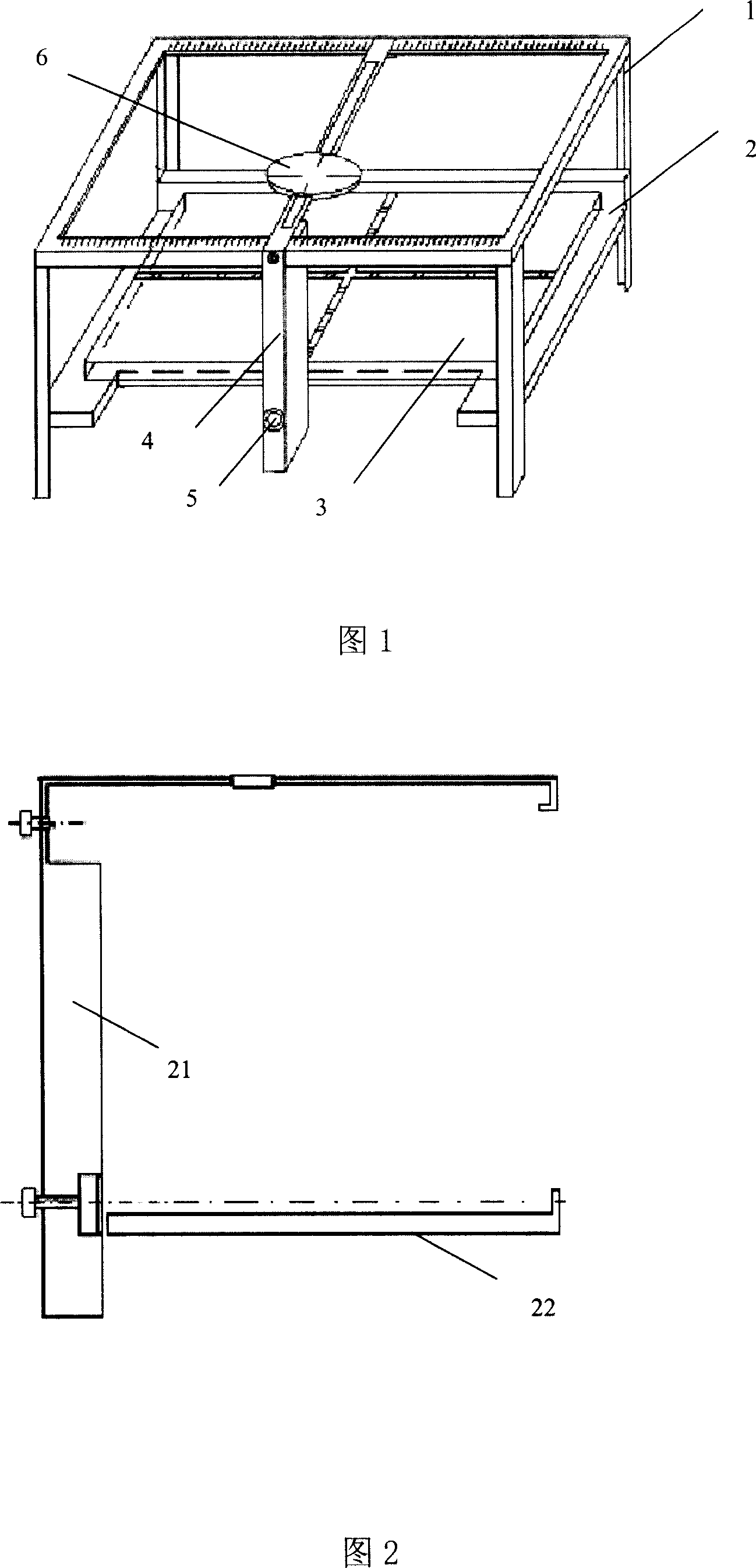
[0030] This embodiment includes a device frame, a magnifying glass and its support, a sample stage, a tool frame, and a tool, as shown in FIG. 1 .

[0031] The device frame is divided into two layers, the upper layer is a square frame, and a pair of opposite sides in the frame are engraved with scales, which can be inserted into the upper inner recess of the tool frame as a guide rail when the tool frame moves.

[0032] The four corners of the square frame are respectively connected with four legs of the shelf. A sample stage is connected to the leg at a fixed distance from the upper magnifying glass. The distance should ensure that the distance from the upper surface of the sample stage to the upper magnifying glass is the focal length plus the thickness of the wafer.

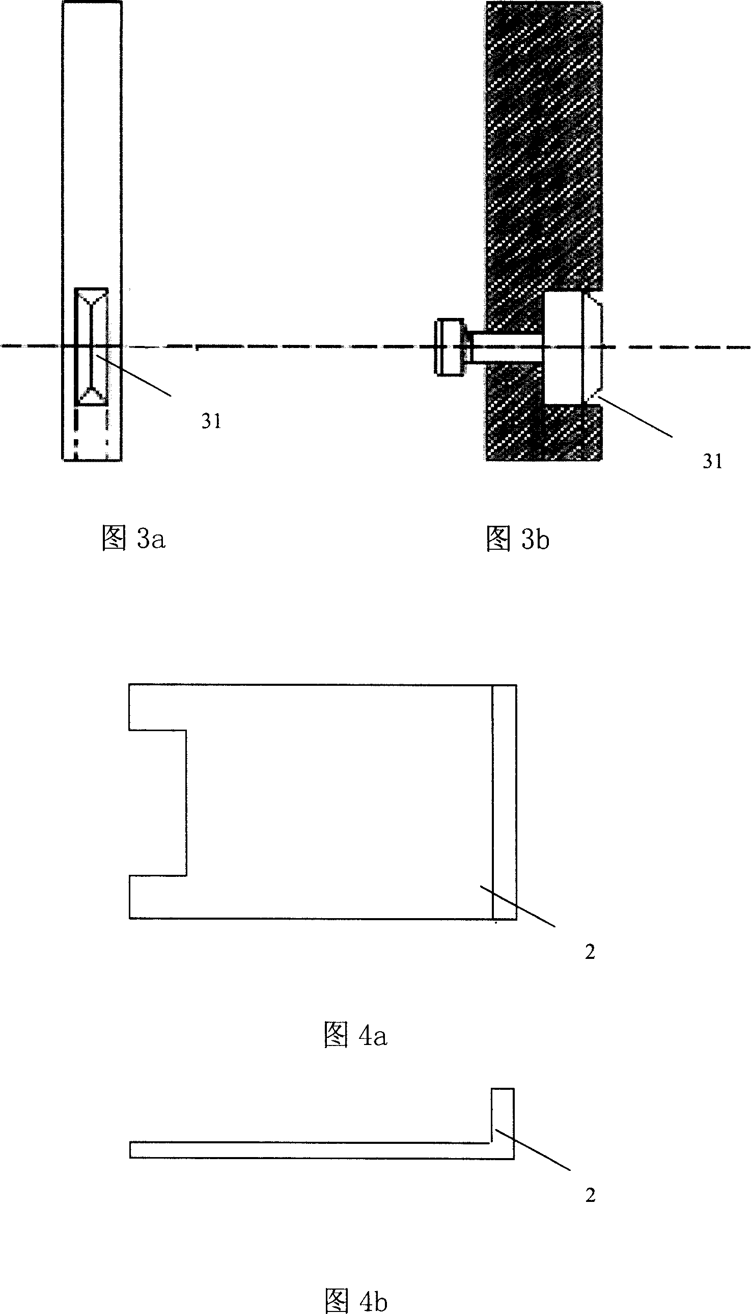
[0033] The top view of the sample stage is shown in Fig. 4a. One side is folded up, and a rectangle is cut in the middle of the other side to prevent the knife from cutting the sample table when entering.

...


PUM


Abstract

Aiming at simply and reliably implementing the precise cutting to the wafer sample testing belt, the invention relates to a cutting tool cutting the wafer sample testing belt and the application method. The cutting tool includes a device frame, a magnifier, a sample table, a cutter rest and a cutter; wherein, the cutter is arranged in the cutter rest, the magnifier and the frame of the magnifier are arranged on the cutter rest, and the sample table is also arranged on the cutter rest.

Description

technical field [0001] The invention relates to a wafer sample cutting tool used in semiconductor production and a using method thereof, in particular to a wafer sample test strip cutting tool and a using method thereof. Background technique [0002] At present, in semiconductor production, there are often microstructure images for testing on the wafer dicing lanes to form test strips. When doing failure analysis, it is often necessary to observe the micro-pattern structure located below the test strip, so it is necessary to cut the test strip structure with a width of about 40-60 microns when cutting the wafer sample. [0003] However, there are problems in the two cutting methods commonly used in the current cutting method. [0004] One way to cut is to use visual inspection to locate and then cut the test strip in half by hand using a diamond-tipped cutting pen. In this way, the operator cannot well grasp the magnitude of the force and the depth of the cut, and the nake...

Claims


Application Information

Patent Timeline
IPC IPC(8): B28D5/04
Inventor 葛挺锋陈险峰陈强邹丽君
Owner SEMICON MFG INT (SHANGHAI) CORP
Why Eureka
Try Eureka