Program code memory bank in processor piece based on FLASH structure and method for realizing execution in code piece

A program code and processor technology, applied in memory systems, program control devices, electrical digital data processing, etc., can solve the problems of large area, high NORFLASH cost, small capacity, etc., achieve small size, improve reading speed, and facilitate The effect of encapsulation and integration

Active Publication Date: 2008-01-30
HANGZHOU SYNOCHIP DATA SECURITY TECH CO LTD
View PDF0 Cites 15 Cited by
  • Summary
  • Abstract
  • Description
  • Claims
  • Application Information

AI Technical Summary

Problems solved by technology

[0008] In order to solve the above problems, the purpose of the present invention is to integrate NAND FLASH into the processor as the internal memory of the processor, which solves the shortcomings of the existing solution NOR FLASH, such as high cost, large area, and small capacity, and provides a FLASH architecture-based Processor on-chip program code storage body, and method for implementing on-chip execution (XIP) of program code stored in NAND FLASH

Method used


Image

  • Program code memory bank in processor piece based on FLASH structure and method for realizing execution in code piece
  • Program code memory bank in processor piece based on FLASH structure and method for realizing execution in code piece
  • Program code memory bank in processor piece based on FLASH structure and method for realizing execution in code piece

Examples


Embodiment Construction

[0054] The present invention will be further described below in conjunction with the accompanying drawings.

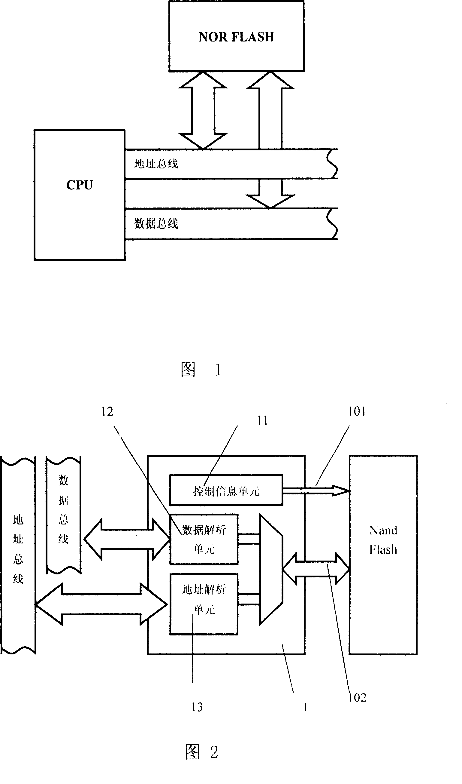
[0055] See Figure 1 for the connection between the CPU and NOR FLASH. In the prior art, the internal program / data of the processor is stored in NOR FLASH. Nor Flash has an independent data bus and address bus, which are directly connected to the data and address of the processor. connected to the bus interface.

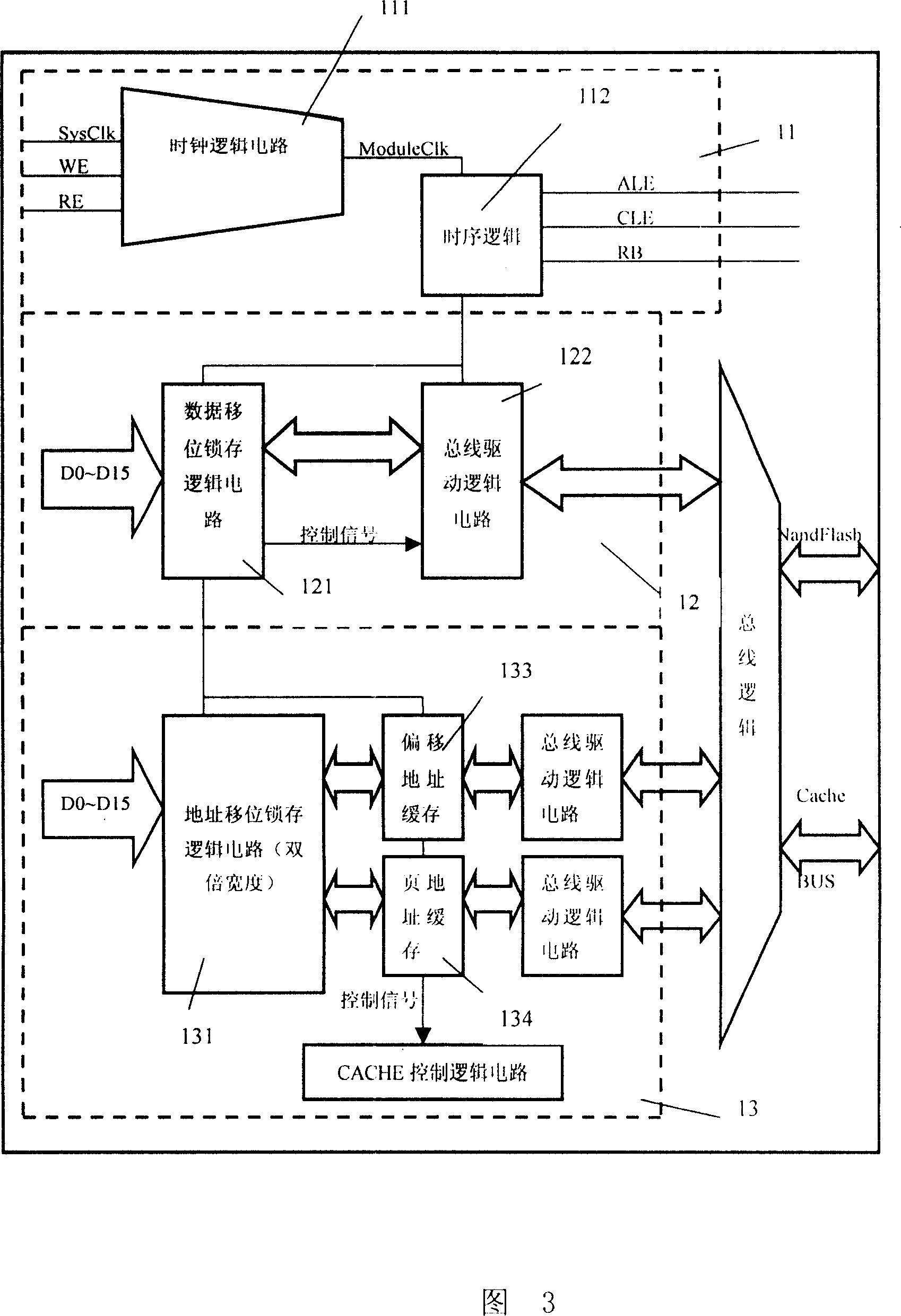
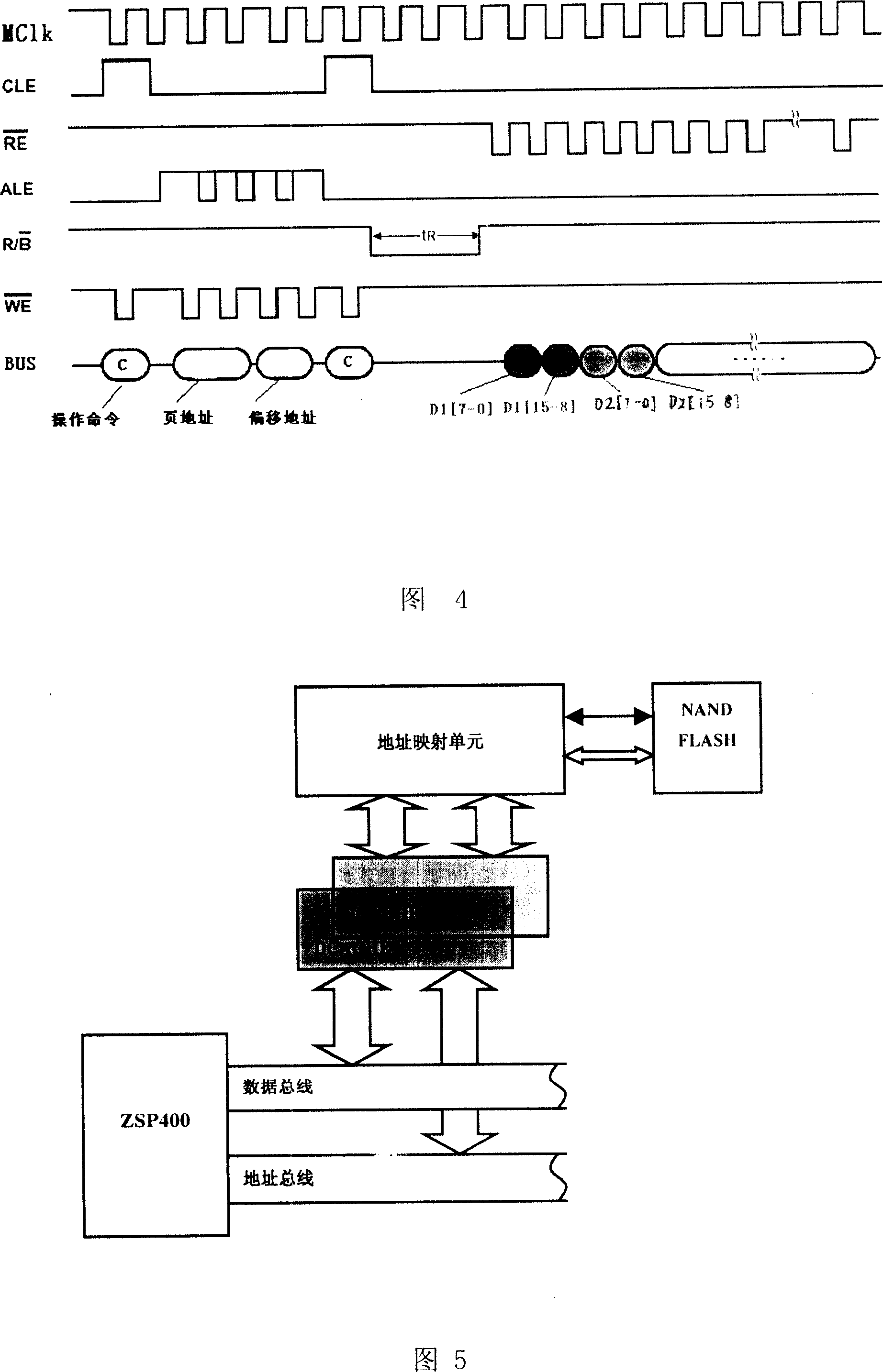
[0056] In order to realize the NAND FLASH as the on-chip storage body of the processor and realize the code on-chip execution, the present invention converts the linear address and the NAND FLASH index type address through the address mapping unit. Using the address mapping unit, the program code stored in NAND FLASH can be implemented on-chip (XIP). NAND FLASH uses the index address of page number + page offset. This address structure is different from the linear address used when the CPU fetches instructions. If conversion is not performed, the CPU cannot ...


PUM


Abstract

A processor on-chip program code memory that is based on a FLASH framework and a method that realizes the execution of the on-chip code belongs to the chip technical field, which is characterized in that the FLASH is in the form of NAND, and the memory comprises an address mapping unit which is logically arranged between the CPU and the NAND FLASH for the conversion between an indexed address of the NAND FLASH and a linear address. The invention leads the program code to be stored in the NAND FLASH to realize the on-chip execution (XIP) by the address mapping unit, and solves the disadvantages of the prior NOR FLASH such as high cost, large area and small capacity. By taking the NAND FLASH as the memory of the processor, the invention breaks the limitations for capacity, and the small volume is convenient for the packaging and integration with a high speed of erasure and more erasing times.

Description

technical field [0001] The invention belongs to the technical field of a system chip (SOC), and in particular relates to a program code storage body in a processor chip based on a FLASH architecture and a method for realizing code chip execution. Background technique [0002] Flash memory (Flash Memory) is called FLASH for short, and it is a kind of non-volatile memory NVM (Non-Volatile Memory). Its characteristic is that it can still maintain on-chip information when the power supply is turned off. According to different technical architectures, flash memory in the world is mainly divided into two types: NOR architecture (Nor Flash) and NAND architecture (Nand Flash). [0003] The biggest feature of Nor Flash is that it has an independent data bus and address bus, which can be read quickly and randomly, allowing the system to read code directly from Flash for execution, that is, execute on-chip (XIP, eXecuteIn Place), so that applications can be directly stored in the flash...

Claims


Application Information

Patent Timeline
Patent Type & Authority Applications(China)
IPC IPC(8): G06F13/00G06F9/445G06F12/08G06F12/0873
Inventor 裴育
Owner HANGZHOU SYNOCHIP DATA SECURITY TECH CO LTD
Why Eureka
Try Eureka