Electronic device and manufacturing method thereof

The technology of an electronic device and manufacturing method is applied in the fields of printed circuit manufacturing, printed circuit, electrical components, etc., and can solve problems such as the inability to reduce the thickness of the electronic device, the cost, and the inability to effectively use the space of the electronic device, so as to improve the yield rate and reduce the material Cost, effective thinning effect

Active Publication Date: 2008-01-30
LITE ON OPTO TECH (CHANGZHOU) CO LTD +1
View PDF0 Cites 15 Cited by
  • Summary
  • Abstract
  • Description
  • Claims
  • Application Information

AI Technical Summary

Problems solved by technology

Therefore, additional costs are incurred in material costs and man-hours for manufacturing and assembling
Moreover, the antenna carrier has a certa

Method used


Image

  • Electronic device and manufacturing method thereof
  • Electronic device and manufacturing method thereof
  • Electronic device and manufacturing method thereof

Examples


Embodiment Construction

[0036] In order to make the above and other objects, features and advantages of the present invention more comprehensible, the preferred embodiments are specifically cited below, together with the accompanying drawings, and are described in detail as follows:

[0037] In the following, the present invention will be described in detail with examples and drawings. In the drawings or descriptions, similar or identical parts use the same symbols. In the drawings, the shapes or thicknesses of the embodiments may be exaggerated for simplification or convenient labeling. Part of the elements in the drawings will be described in the description. It is to be understood that elements not shown or described may have various forms known to those skilled in the art. In addition, when it is stated that a layer is on a substrate or another layer, the layer may be directly on the substrate or another layer, or there may be an intervening layer therebetween.

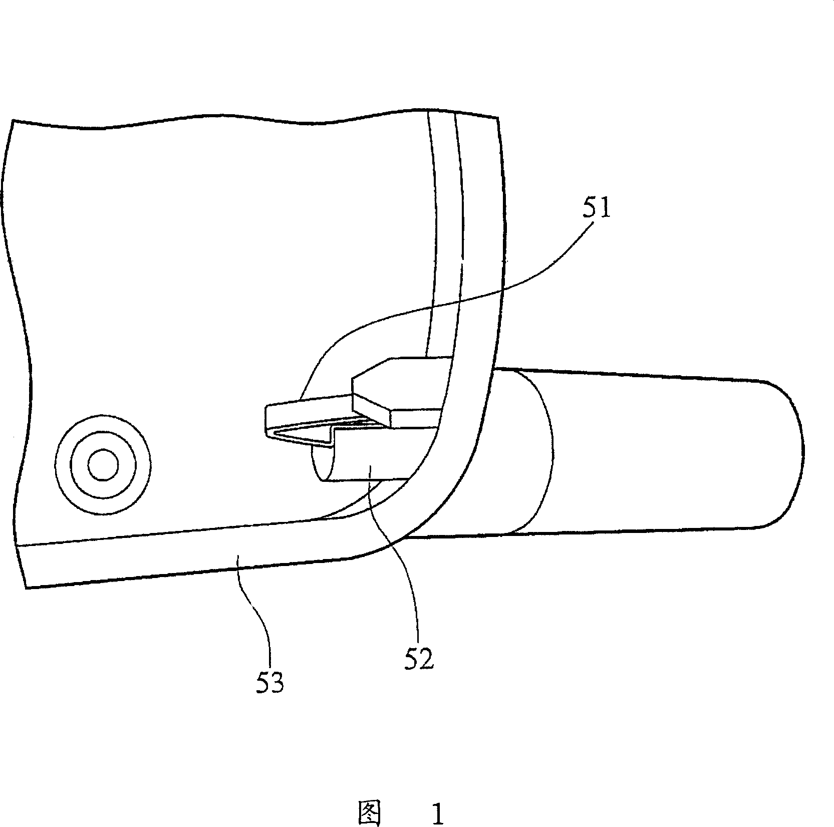
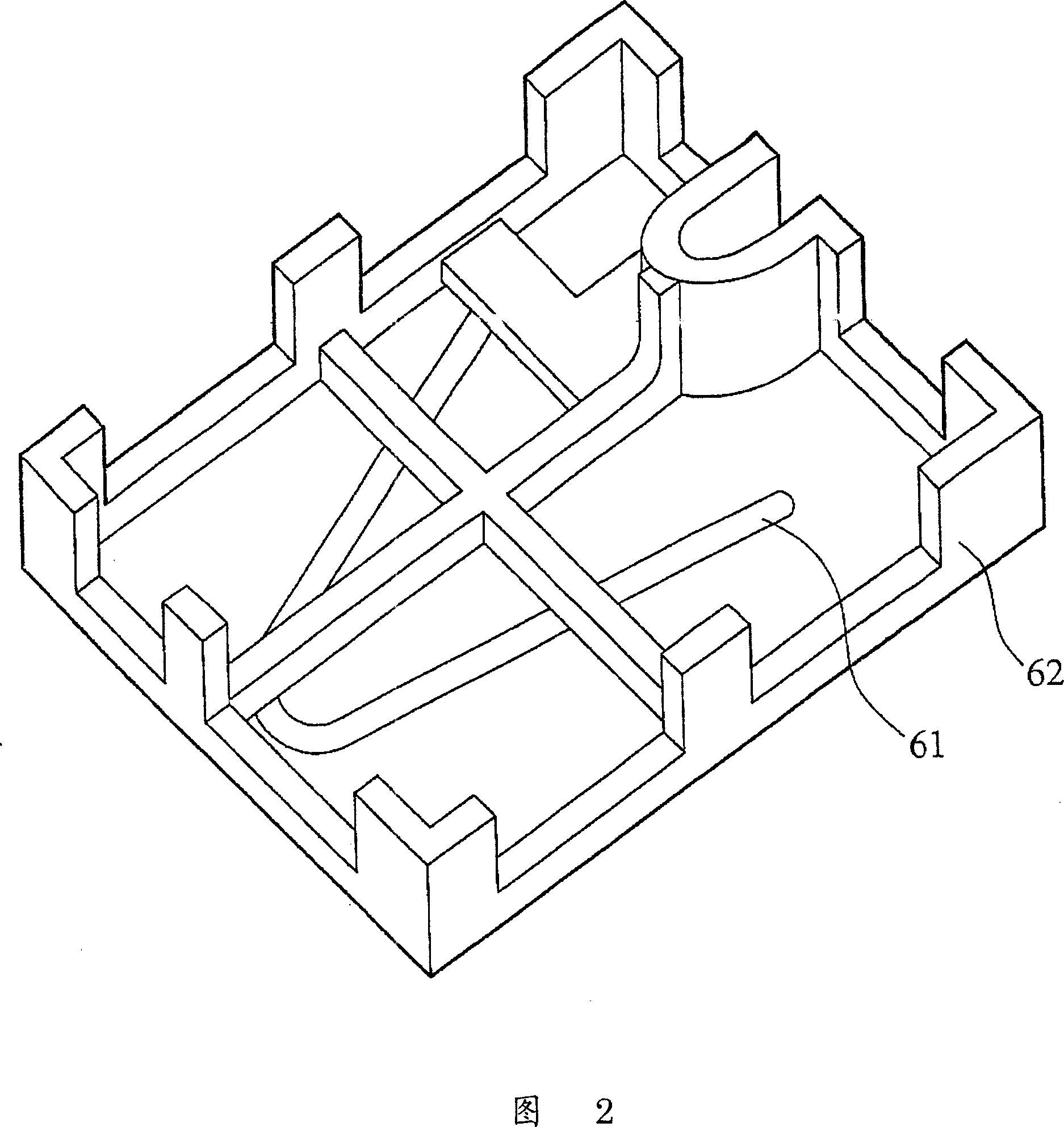
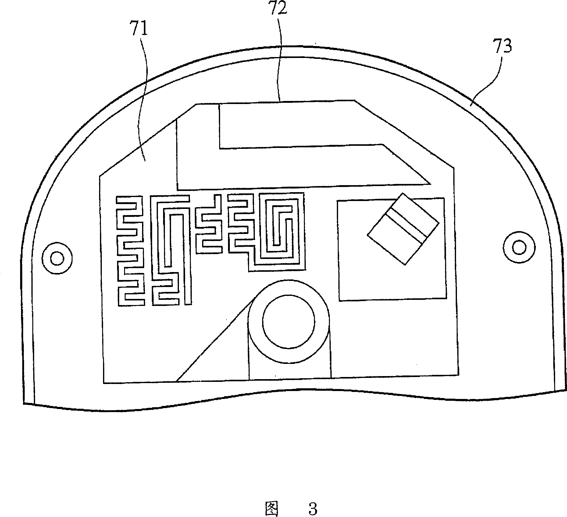
[0038] Please refer to FIG. 5 a...


PUM

PropertyMeasurementUnit
Resistanceaaaaaaaaaa

Abstract

The invention provides an electronic device and a manufacture method of the electronic device. The electric device comprises a substrate and a pattern conducting layer which is formed on the external surface of the substrate as an antenna layer and is electrically connected with a controlling circuit board to send or receive a wireless signal, wherein the substrate is positioned between the pattern conducting layer and the controlling circuit board. The pattern conducting layer can be electrically connected with the controlling circuit board through a hole by using a spring sheet to send/receive wireless signals. The substrate can be a shell of the electronic device. The electronic device and the manufacture method of the invention can reduce materials cost, increase the coherence of the electronic device assembly and effectively thin the electronic device.

Description

technical field [0001] The present invention relates to an electronic device, in particular to an electronic device with a patterned conductive layer as an antenna layer. Background technique [0002] The antenna is a part that performs electromagnetic conversion on radio transmitting and receiving equipment. In handheld electronic products, antennas are generally divided into two categories: exposed and hidden. Please refer to FIG. 1 to FIG. 4 , which are antenna designs of known electronic devices. As shown in FIG. 1 , the exposed antenna 51 is disposed on the antenna carrier 52 , and the antenna 51 protrudes from the housing 53 of the electronic device. And the design of common concealed antenna has following several kinds at present: one, as shown in Figure 2, after stamping iron plate, to form an antenna 61, then antenna 61 is arranged on an antenna carrier 62, is installed on at last again Inside the electronic device; two, as shown in Figure 3, the antenna layer is...

Claims


Application Information

Patent Timeline
IPC IPC(8): H01Q1/38H01Q1/40H05K3/00
Inventor 李德威
Owner LITE ON OPTO TECH (CHANGZHOU) CO LTD
Why Eureka
Try Eureka