Element calling system and method

A technology for components and electronic components, applied in the field of component calling systems, can solve the problems of wasting the precious time of electronic engineers, spending too long, and low work efficiency, and achieve the effect of shortening research and development time, reducing layout work time, and improving work efficiency.

Inactive Publication Date: 2008-02-06
INVENTEC CORP
View PDF0 Cites 6 Cited by
  • Summary
  • Abstract
  • Description
  • Claims
  • Application Information

AI Technical Summary

Problems solved by technology

However, in the process of arranging electronic components, the above-mentioned component layout operations are usually carried out sequentially according to the distribution of the lines (net) in the circuit schematic diagram. For a certain circuit, when looking for the required electronic component data in the circuit schematic diagram containing thousands of electronic components and placing them on the printed circuit board one by one, it is very easy to cause errors in the placement of electronic components and often take too long It takes time to find the required electronic components and place them on the correct position of the printed circuit board among the many electronic component data of the same type that are piled up together. This will inevitably reduce the work efficiency of electronic component layout operations and waste the precious time of electronic engineers. time
Furthermore, because the types of electronic components are increasing day by day and are very similar, if an electronic engineer wants to modify or replace the electronic components in the original circuit diagram, it is impossible to immediately find the required electronic components for replacement in a large number of electronic component data. In this way, the development time will be extended gradually
[0004] As mentioned above, how to solve the lack of low work efficiency caused by electronic engineers spending too much time looking for electronic components in the existing electronic component layout technology has become an urgent technical problem to be solved

Method used


Image

  • Element calling system and method
  • Element calling system and method

Examples


Embodiment Construction

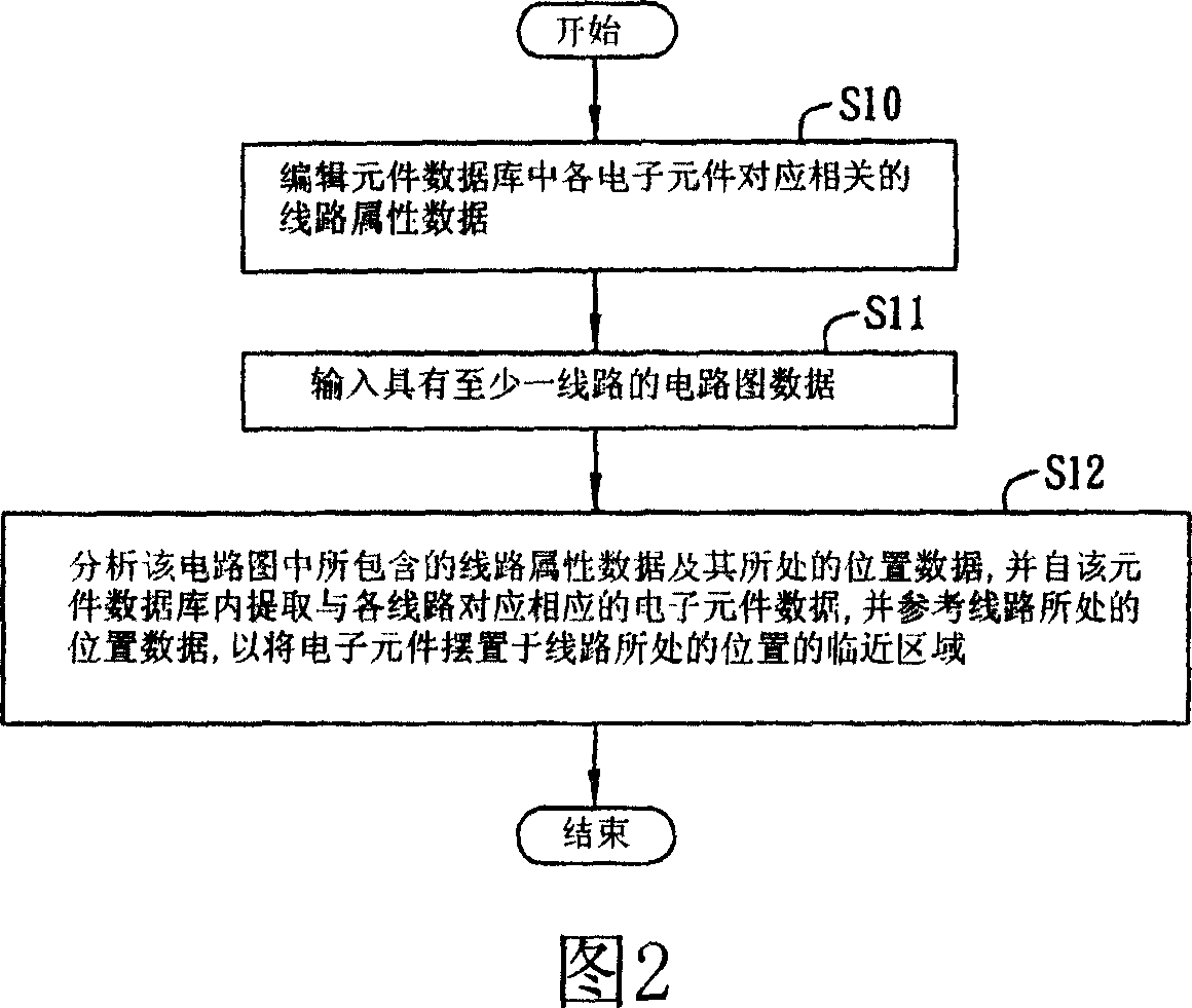
[0030] The implementation of the present invention is illustrated through specific specific examples below, and those skilled in the art can easily understand other advantages and effects of the present invention from the content disclosed in this specification. The present invention can also be implemented or applied through other different specific examples, and various modifications and changes can be made to the details in this specification based on different viewpoints and applications without departing from the spirit of the present invention.

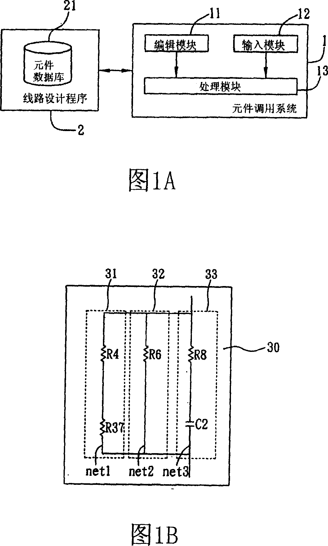
[0031] Please refer to FIGS. 1A-1B , which are used to show the schematic structure of the component calling system 1 of the present invention. As shown in FIG. 1A , the component invoking system 1 of the present invention is mounted on a circuit design program 2 to assist the circuit design program 2 in performing electronic component layout operations. Furthermore, the circuit design program 2 has a component database 21 for s...


PUM


Abstract

The present invention relates to a component calling system and method. The present invention carries to a circuitry design program to aid the circuitry design program to implement the electronic element layout job, the circuitry design program has a component database used for storing electronic component data, firstly, the circuitry property data relative to each electronic element in the component database is edited through an editing module, secondly, an input interface provided via an input module inputs the circuit diagram data possessed with at least one circuitry, lastly, a processing module is enabled to analyze the circuitry property data contained in the circuit diagram data input by the input module and the location data, and according to the circuitry property data relative to each electronic component edited by the editing module, the electronic component data relative to the circuitry is withdrawn from the component database, and with reference to the location data of the circuitry, the withdrawn electronic component data is put in the area near the location, so as to provide the circuitry design program to implement the subsequent electronic component layout job, thus rapidly realizing the layout job of the electronic component, thereby the efficiency of the layout job of the electronic component can be improved.

Description

technical field [0001] The present invention relates to a component calling system and method, more specifically, to a component calling system and method for assisting a circuit design program in executing wiring operations. Background technique [0002] Nowadays, electronic engineers usually design printed circuit boards through various circuit design programs (such as Protel software). The design process is to first design the corresponding circuit schematic diagram through a circuit design program according to actual needs, and then design The schematic circuit diagram file is converted into a layout diagram file for subsequent electronic component layout operations. [0003] Usually, when doing electronic component layout work, the electronic engineer will first transfer all kinds of electronic component data contained in the circuit schematic diagram into the layout file generated by the conversion. The specific method is to make the circuit design program according to...

Claims


Application Information

Patent Timeline
IPC IPC(8): G06F17/50
Inventor 范文纲伍会意
Owner INVENTEC CORP
Why Eureka
Try Eureka