And/not gate type non-volatility memory and manufacturing method and operation method therefor

A non-volatile, manufacturing method technology, applied in the direction of static memory, read-only memory, semiconductor/solid-state device manufacturing, etc., can solve the problems of reading interference and taking a long time, and achieve the effect of reducing coupling interference

Inactive Publication Date: 2008-02-06
POWERCHIP SEMICON CORP
View PDF0 Cites 13 Cited by
  • Summary
  • Abstract
  • Description
  • Claims
  • Application Information

AI Technical Summary

Problems solved by technology

In this way, in the programming operation of the existing NAND type non-volatile memory, it is necessary to perform multiple programming steps and programming confirmation steps, so that the programmed memory cells are accurately set in the initial voltage, so that the take a long time
Moreover, when a selected memory cell is read, other non-selected memory cells in the same memory cell column are likely to cause read interference to the selected memory cell.

Method used


Image

  • And/not gate type non-volatility memory and manufacturing method and operation method therefor
  • And/not gate type non-volatility memory and manufacturing method and operation method therefor
  • And/not gate type non-volatility memory and manufacturing method and operation method therefor

Examples


Embodiment Construction

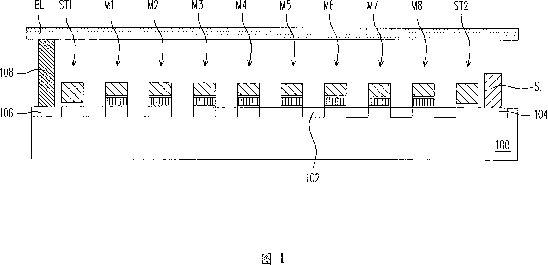
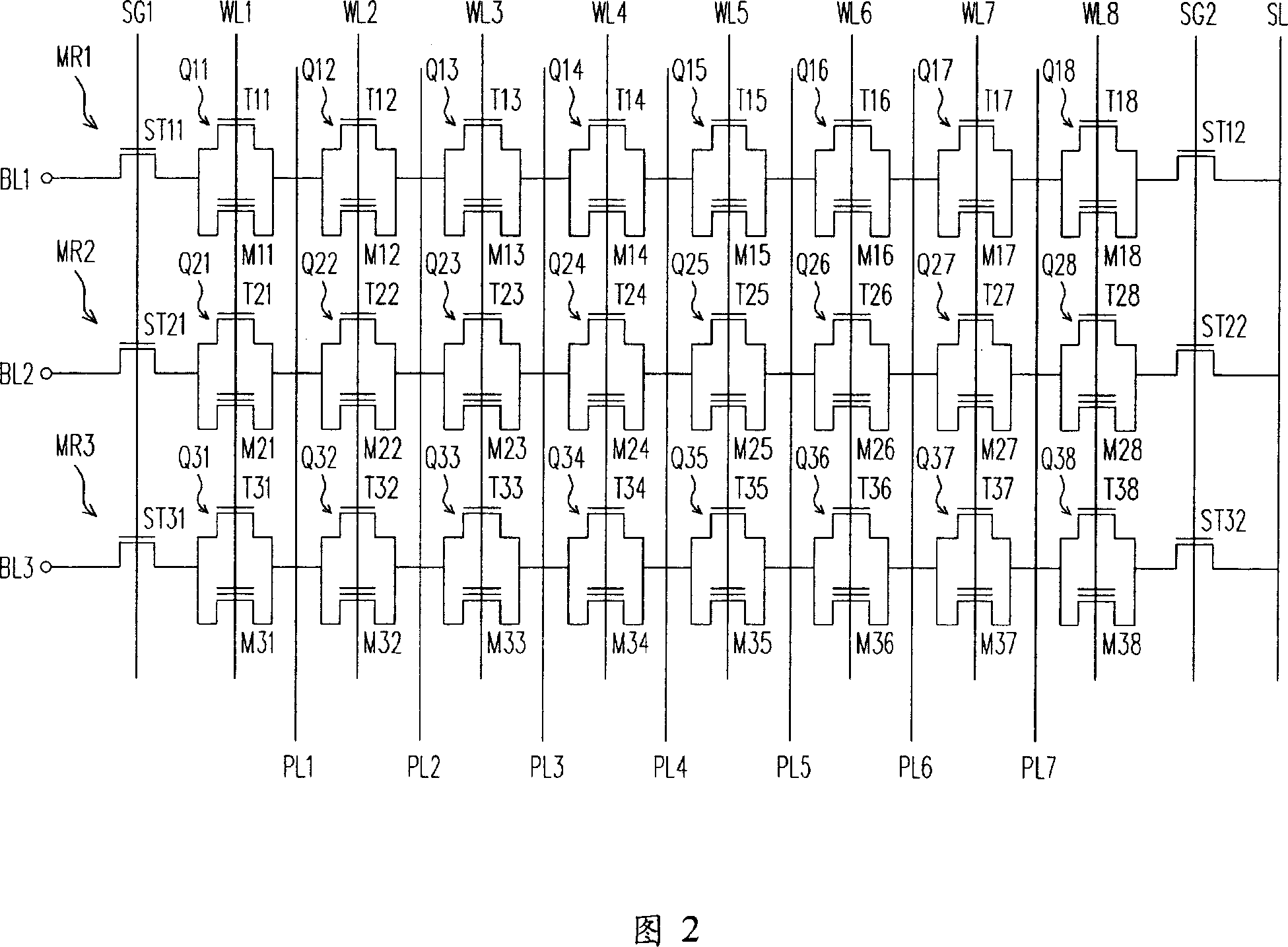
[0100] FIG. 2 is a schematic circuit diagram showing a NAND (NAND) type non-volatile memory array of the present invention. In this embodiment, a row of 8 memory cells and a total of three rows of NAND memory cells are taken as an example for illustration.

[0101] Please refer to FIG. 2, the NAND (NAND gate) type non-volatile memory array includes a plurality of selection transistors ST11-ST31 and ST12-ST32, a plurality of memory cells Q11-Q38, a plurality of word lines WL1-WL8, and selection gate lines SG1 and SG2 , bit lines BL1 - BL3 and pass gate lines PL1 - PL7 .

[0102] Memory cells Q11 to Q18 are connected in series between selection transistor ST11 and selection transistor ST12 to form a memory cell row MR1 in the row direction. The memory cells Q21 to Q28 are connected in series between the selection transistor ST21 and the selection transistor ST22 to form a memory cell row MR2 in the row direction. The memory cells Q31 to Q38 are connected in series between the ...


PUM


Abstract

A non-logic gate and non-volatile memory has a plurality of memory cell rows; each memory cell row includes a source region and a drain region, a plurality of memory cells, a plurality of transmission grids, a first selection transistor and a second selection transistor; wherein, the source region and the drain region are arranged in a base board, a plurality of memory cells are positioned on the base board between the source region and the drain region, and each memory cell comprises a memory cell and a transistor, and the memory cell is connected with the transistor in parallel. Moreover, the transmission grids are respectively mounted on the base board between two neighboring memory cells and connect the memory cells in series, and the first selection transistor and the second selection transistor are respectively connected with two memory cells outside and are respectively next to the source region and the grain region.

Description

technical field [0001] The invention relates to a semiconductor element, in particular to a NAND gate (NAND) type non-volatile memory and its manufacturing method and operation method. Background technique [0002] Non-volatile memory elements have been widely used in personal computers and electronic devices due to their advantages of multiple data storage, reading, and erasing, and the stored data will not disappear after power off. a memory element. [0003] A typical non-volatile memory device is generally designed to have a stacked gate (Stacked-Gate) structure, which includes a floating gate (Floating Gate) and a control gate (Control Gate) made of doped polysilicon. The floating gate is located between the control gate and the substrate, and is in a floating state, not connected to any circuit, while the control gate is connected to the word line (Word Line), and also includes the tunnel oxide layer (Tunneling Oxide) and an inter-gate dielectric layer (Inter-Gate Di...

Claims


Application Information

Patent Timeline
IPC IPC(8): H01L27/115H01L23/522H01L21/8247H01L21/768G11C16/02
Inventor 郭兆玮赵志明黄汉屏魏鸿基毕嘉慧
Owner POWERCHIP SEMICON CORP
Why Eureka
Try Eureka