Method for solving damage of metal oxide semiconductor (MOS) caused by highly rapid load change of voltage regulator (VR)

A technology for changing loads and switching chips, which is applied in the direction of output power conversion devices, measuring devices, electrical components, etc. It can solve problems such as abnormal chip feedback voltage, large coupling interference, and MOS damage, and achieve operational data processing and safe data processing. , Reduce the effect of coupling interference

Inactive Publication Date: 2016-01-06
LANGCHAO ELECTRONIC INFORMATION IND CO LTD
View PDF5 Cites 3 Cited by
  • Summary
  • Abstract
  • Description
  • Claims
  • Application Information

AI Technical Summary

Problems solved by technology

Due to the effect of the output inductance, the faster the MOS switching frequency, the higher the PHASE voltage generated after the upper MOS is turned on, and the greater the coupling interference generated on the GND inside the chip; when the coupling interference on the GND reaches about 2.5V , it may cause the feedback voltage read inside the chip to be abnormal, resulting in logic errors
As a result, the upper and lower MOSs are turned on at the same time, and a short circuit burns the MOS.
[0006] In order to prevent this from happening, this article proposes a design method to solve the problem of MOS damage caused by too fast VR load changes. By adding a resistor between PHASE and GND, it is used for filtering and reduces coupling interference.

Method used


Image

  • Method for solving damage of metal oxide semiconductor (MOS) caused by highly rapid load change of voltage regulator (VR)
  • Method for solving damage of metal oxide semiconductor (MOS) caused by highly rapid load change of voltage regulator (VR)
  • Method for solving damage of metal oxide semiconductor (MOS) caused by highly rapid load change of voltage regulator (VR)

Examples


Embodiment Construction

[0020] The present invention will be further described below in conjunction with the accompanying drawings and specific embodiments.

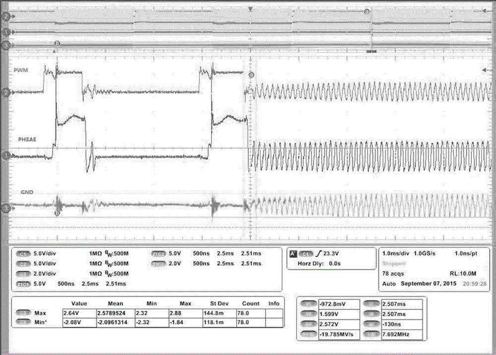
[0021] The present invention provides a method for solving the problem of MOS damage caused by too fast VR load changes, breaks the fixed configuration of the original server collocation, and more widely supports the design concept of larger data processing volume and faster load change rate. And adopt a new idea: no matter what type of network card, hard disk, etc. the server motherboard is equipped with, the server motherboard can support it, and it will no longer be affected by the excessively fast load change rate during the processing of large amounts of data, resulting in crashes. In this way, the application of server motherboards is wider (lower requirements than server motherboards with fixed configurations), and it can meet the application needs of different users to a greater extent.

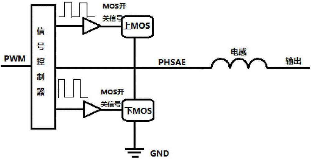
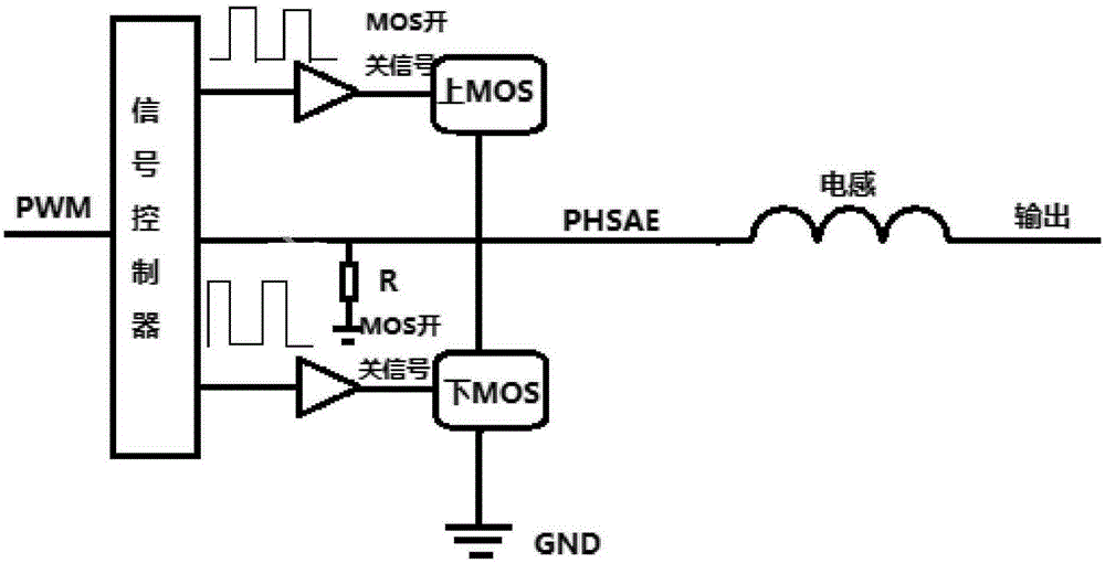
[0022] Its specific implementation process is: ...


PUM


Abstract

The invention discloses a method for solving damage of a metal oxide semiconductor (MOS) caused by a highly rapid load change of a voltage regulator (VR). The method is achieved according to the following steps that in a power supply conversion chip of a server mainboard, mistaken receiving of a feedback signal by the chip is prevented by reducing the internal coupling interference of the power supply conversion chip when the load change rate is too fast, an internal logical error is further prevented from occurring, the MOS is ensured to normally work during the conversion process, and an output voltage is in a normal application range. Compared with the prior art, the method for solving the damage of the MOS caused by the highly rapid load change of the VR has the advantages that: aiming at the problem of MOS burnout caused by the highly rapid load change when the server mainboard is matched in different configurations or in different working modes, and a fault is prevented from occurring in a product during the working process and affecting normal working; and meanwhile, the method is also applicable for improving the working stability of various server circuit board cards, is high in practicability and is easy to promote.

Description

technical field [0001] The invention relates to the technical field of computer servers, in particular to a method that has strong practicability and solves the problem of MOS damage caused by rapid VR load changes. Background technique [0002] When working on server designs, we will find that large server motherboard designs have a lot of voltage conversion. Including: before power-on, normal start-up operation and after system shutdown. For any state, usually, there will be different conversion circuits during the design process, which can not only save energy but also ensure the maximum efficiency, and also prevent uncertain factors in the working process of the board from causing damage to the board. And the VR (Voltage Regulator, ie: voltage converter) on our main board will change the load at different rates according to the different application requirements after normal startup and operation, and the MOS switching frequency during the voltage conversion process wil...

Claims


Application Information

Patent Timeline
Patent Type & Authority Applications(China)
IPC IPC(8): H02M1/32H02M1/38H02M1/44G06F1/26
Inventor 曹先帅
Owner LANGCHAO ELECTRONIC INFORMATION IND CO LTD
Why Eureka
Try Eureka