
Method for preparing nano silicon-base porous luminescent material by normal pressure plasma gas phase deposition
A normal-pressure plasma, luminescent material technology, applied in luminescent materials, chemical instruments and methods, metal material coating technology, etc., can solve the problem of large electron mean free path, difficult to apply other matrix materials, difficult to give full play to porous silicon nanomaterials Quantum confinement effect and surface effect, etc., to achieve the effect of improving quantum luminous efficiency, strong fluorescence, and uniform deposition effect
- Summary
- Abstract
- Description
- Claims
- Application Information
AI Technical Summary
Problems solved by technology
Method used
Image

Examples
Embodiment 1
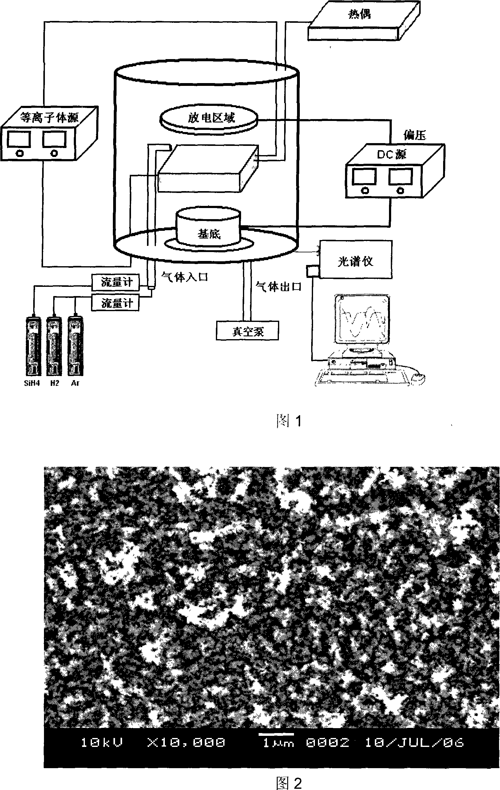
[0033] The deposition substrate is made of glass sheet, which is ultrasonically cleaned with ethanol and deionized water, and placed in a plasma reactor. The electrode is a tungsten wire with a diameter of 0.1 mm, and is covered with a quartz tube. The number of electrodes is 12, 5 layers, and the distance between electrodes and the distance between layers Both are 5mm, the distance between the substrate and the discharge area is 0.3cm, and the vacuum is evacuated to the background vacuum degree ≤ 10 3 After Pa, pass into the mixed gas containing silane, argon, hydrogen, the ratio is: silane: argon: hydrogen = 4: 95: 1, adjust the flow rate to be 140SCCM, control the vacuum degree of 1.05 * 10 5 Pa, opening frequency 2×10 4 Hz plasma power supply, controlled discharge power of 5W, bias voltage of 100V, pulse ratio of 90%, and discharge time of 10 minutes.
[0034] After deposition, the glass slide was detected by high-resolution transmission electron microscope SEM. The resul...
Embodiment 2
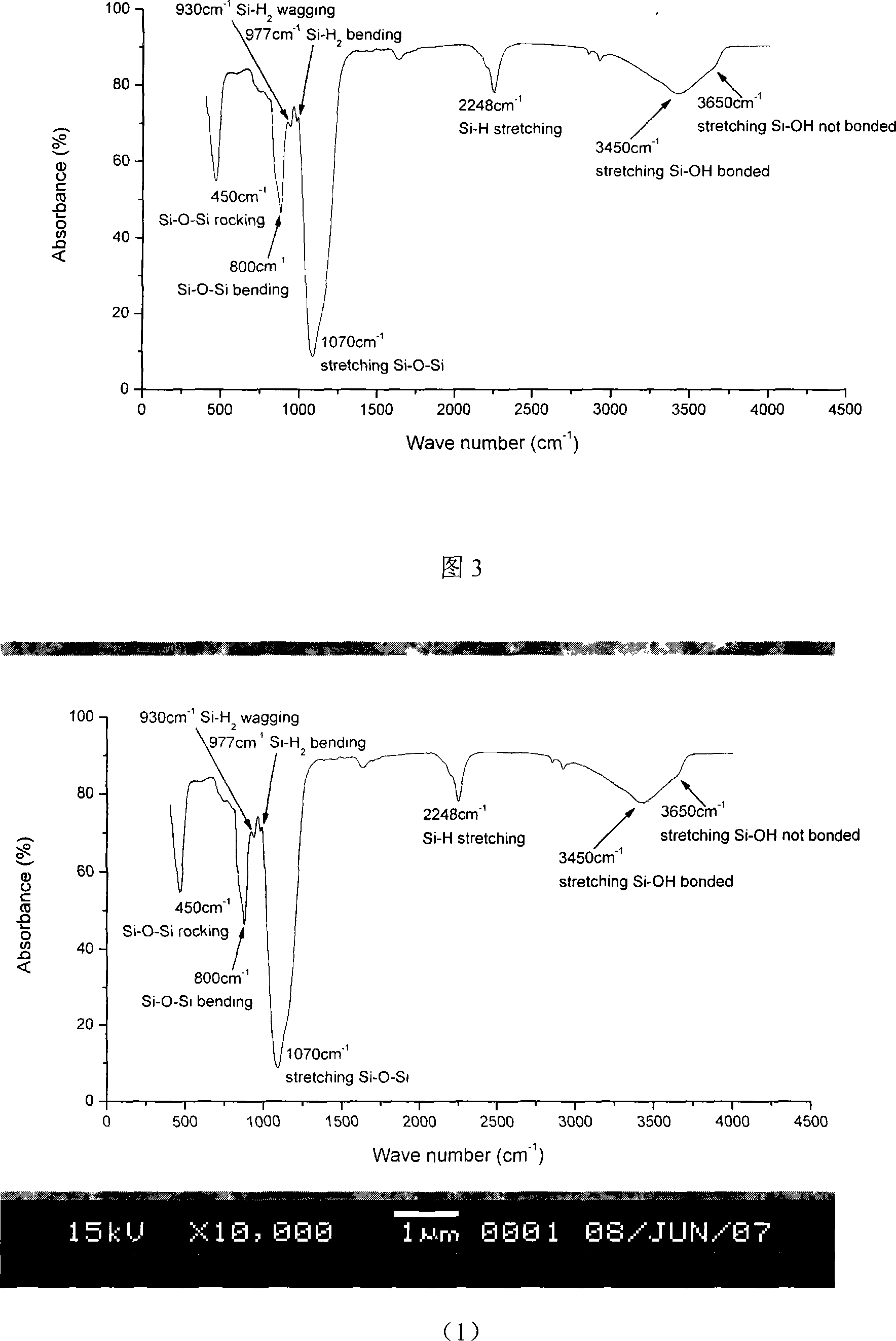
[0036] The deposition substrate is made of silicon polyester sheet. After ultrasonic cleaning with ethanol and deionized water, it is placed in a plasma reactor. The electrodes are made of stainless steel with a diameter of 3 mm and are covered with alumina ceramic tubes. The number of electrodes is 8, 2 layers, and the distance between electrodes is the same as The distance between layers is 3mm, the distance between the substrate and the discharge area is 0.5cm, and the vacuum is evacuated to the background vacuum degree ≤ 10 3 After Pa, pass into the mixed gas containing silane, argon, hydrogen, the ratio is: silane: helium: hydrogen = 1:98:2, adjust the flow rate to be 140SCCM, control the vacuum degree of 1.0×10 5 Pa, opening frequency 2×10 4 Hz plasma power supply, controlled discharge power of 500W, bias voltage of -300V and -850V, pulse ratio of 16%, and discharge time of 3 minutes.
[0037] After the deposition, the polyester sheet was detected by high-resolution tra...
Embodiment 3
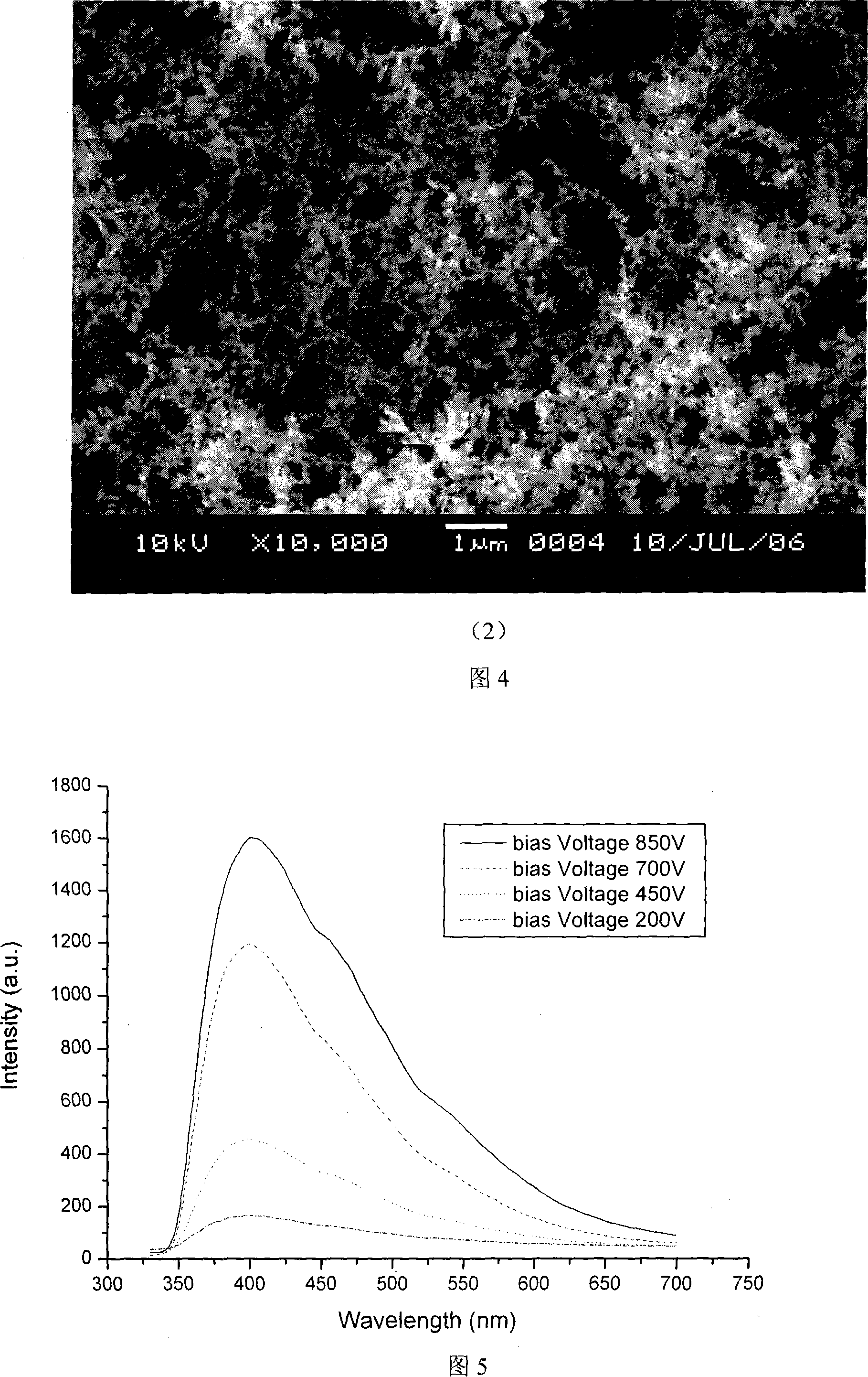
[0039]The deposition substrate is a P-type (100) silicon wafer. After ultrasonic cleaning with ethanol and deionized water, it is placed in a plasma reactor. The inter-layer distance and the inter-layer distance are both 1mm, the distance between the substrate and the discharge area is 0.5cm, and the vacuum is evacuated to a background vacuum degree of ≤10 3 After Pa, pass into the mixed gas containing silane, argon, hydrogen, the ratio is: silane: argon: hydrogen = 1: 89: 10, the adjustment flow rate is 140SCCM, and the control vacuum is 1.03 × 10 5 Pa, opening frequency 2×10 4 Hz plasma power supply, the control discharge power is 500W, the bias voltages are respectively -200, -450, -700, -850V, the pulse ratio is 16%, and the discharge time is 10 minutes.
[0040] After deposition, the glass slides were detected by laser fluorescence spectroscopy, and the results showed that under the excitation light of 320nm, blue-violet light with a center wavelength of 450nm was emitte...
PUM
| Property | Measurement | Unit |
|---|---|---|
| size | aaaaa | aaaaa |
| size | aaaaa | aaaaa |
| size | aaaaa | aaaaa |
Abstract
Description
Claims
Application Information