Non volatile memory device and its operation method

A non-volatile and memory technology, applied in static memory, read-only memory, digital memory information, etc., can solve the problems of complex and time-consuming programming and writing programs

Inactive Publication Date: 2008-02-13
CONVERSANT INTPROP MANAGEMENT INC
View PDF1 Cites 11 Cited by
  • Summary
  • Abstract
  • Description
  • Claims
  • Application Information

AI Technical Summary

Problems solved by technology

Because data must be transferred between the main register 150 and the auxiliary register 170, the programming an...

Method used


Image

  • Non volatile memory device and its operation method
  • Non volatile memory device and its operation method
  • Non volatile memory device and its operation method

Examples


Embodiment Construction

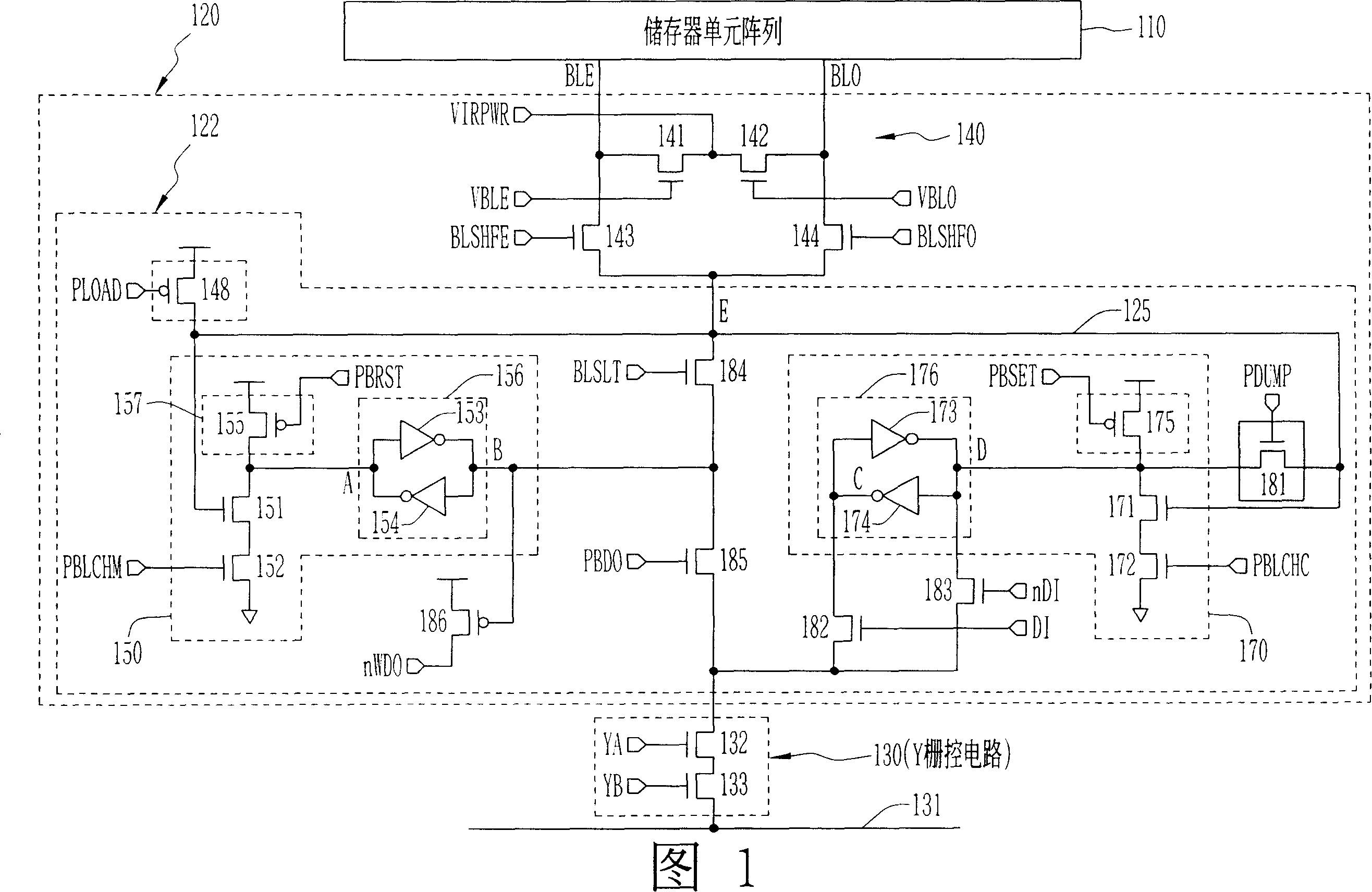
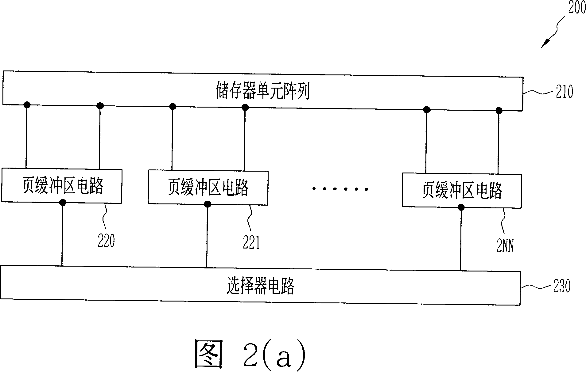
[0037] 2( a ) is a schematic diagram of a flash memory device 200 of the present invention, which includes a memory cell array 210 , a plurality of page buffer circuits 220 , 221 , . . . and 2NN, and a selector circuit 230 . The page buffer circuits 220 , 221 , . . . and 2NN are coupled between the memory cell array 210 and the selector circuit 230 .

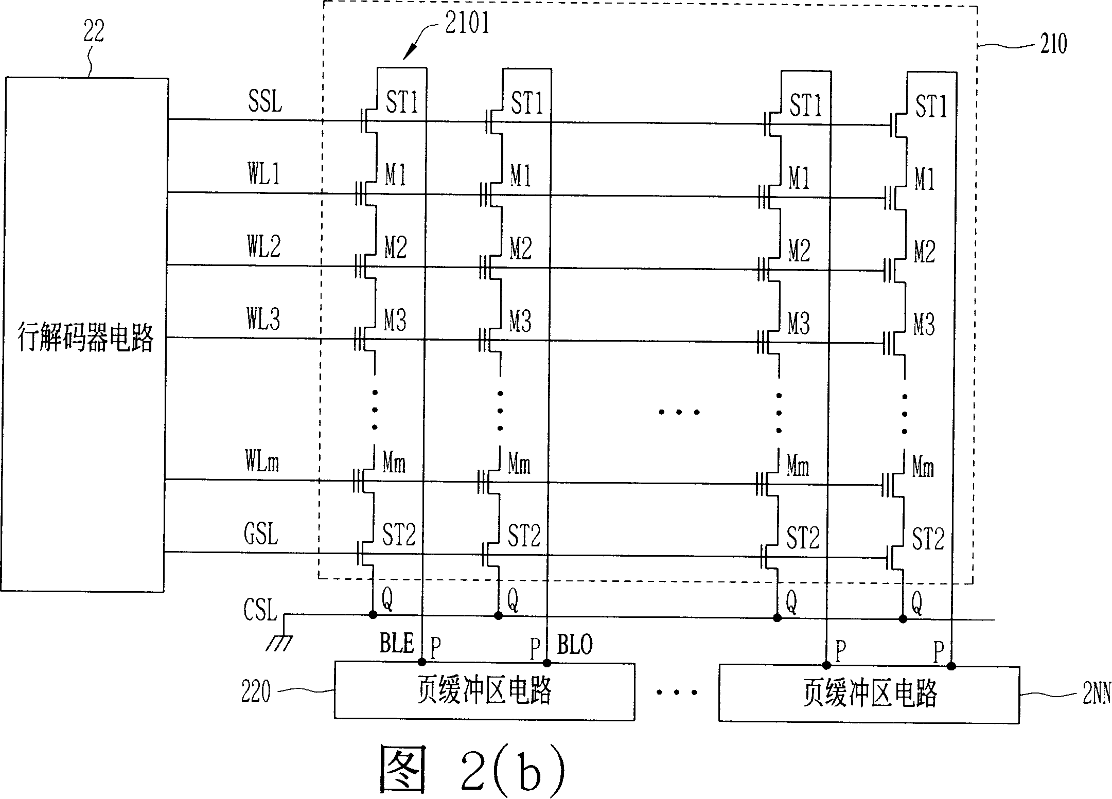
[0038] FIG. 2( b ) is a schematic diagram of the memory cell array 210 according to the first embodiment of the present invention. The memory cell array 210 includes a plurality of cell strings 2101, each of the cell strings 2101 includes a first terminal P and a second terminal Q, and the first terminal P is electrically connected to the corresponding bit line BLE or BLO. The page buffer circuit 220, 221, . . . or 2NN; the second terminal Q is electrically connected to a common source line CSL. The cell string 2101 includes a string selection transistor (string selection transistor) ST1 coupled to the bit line BLE, a ground se...


PUM


Abstract

The invention discloses a nonvolatile memory with the page buffer provided with two resisters, and the memory comprises a memory unit matrix, a selector circuit and a page buffer circuit. The selector circuit is coupled with an outer data bus, the page buffer circuit comprising a first resister and a second resister is coupled between the memory unit matrix and the selector circuit, and the first and the second registers are coupled together via a sensing node. The first and the second registers alternately write the data into the memory unit matrix through programming. When programmed write is carried out for one of the first and the second resisters, the other register is used for storing the data from the data bus at the same time. In other words, when programmed write is being carried out by the first resister, the second memory is used for storing the data from the data bus, and when programmed write is being carried out by the second resister, the first memory is used for storing the data from the data bus.

Description

technical field [0001] The present invention relates to a semiconductor memory device, in particular to a non-volatile memory device with a page buffer circuit having a dual register and an operating method thereof. Background technique [0002] U.S. Patent No. 6,671,204 entitled "Non-Volatile Memory Device with Dual Registers in Page Buffer and Method of Operation Thereof" describes a cache program and copy-back ) function of the page buffer design. FIG. 1 is a schematic diagram illustrating a page register and sense amplifier block 120 . The page register and sense amplifier block 120 is coupled between a memory cell array 110 and a Y gate control circuit 130 . The page register and sense amplifier block 120 includes a bit line control circuit 140 and a page buffer 122 . The page buffer 122 has a sense line 125 connected to the bit line control circuit 140 via a sense node E. As shown in FIG. [0003] The bit line control circuit 140 includes four NMOS transistors 141 ...

Claims


Application Information

Patent Timeline
IPC IPC(8): G11C16/10G11C7/10
Inventor 陈宗仁汪若瑜
Owner CONVERSANT INTPROP MANAGEMENT INC
Why Eureka
Try Eureka