Image sensing part and its making method

A technology of image sensing and components, applied in the direction of electrical components, semiconductor/solid-state device manufacturing, radiation control devices, etc., can solve problems such as hindering the passivation of dangling bonds, achieve good shading effect, and improve the effect of dark current

Active Publication Date: 2011-06-22
UNITED MICROELECTRONICS CORP +1
View PDF0 Cites 0 Cited by
  • Summary
  • Abstract
  • Description
  • Claims
  • Application Information

AI Technical Summary

Problems solved by technology

However, since there is a patterned metal layer 120 for light-shielding, its metal will react with hydrogen gas, hindering the passivation of dangling bonds.
Therefore, there will still be a lot of dark current

Method used


Image

  • Image sensing part and its making method
  • Image sensing part and its making method
  • Image sensing part and its making method

Examples


Embodiment Construction

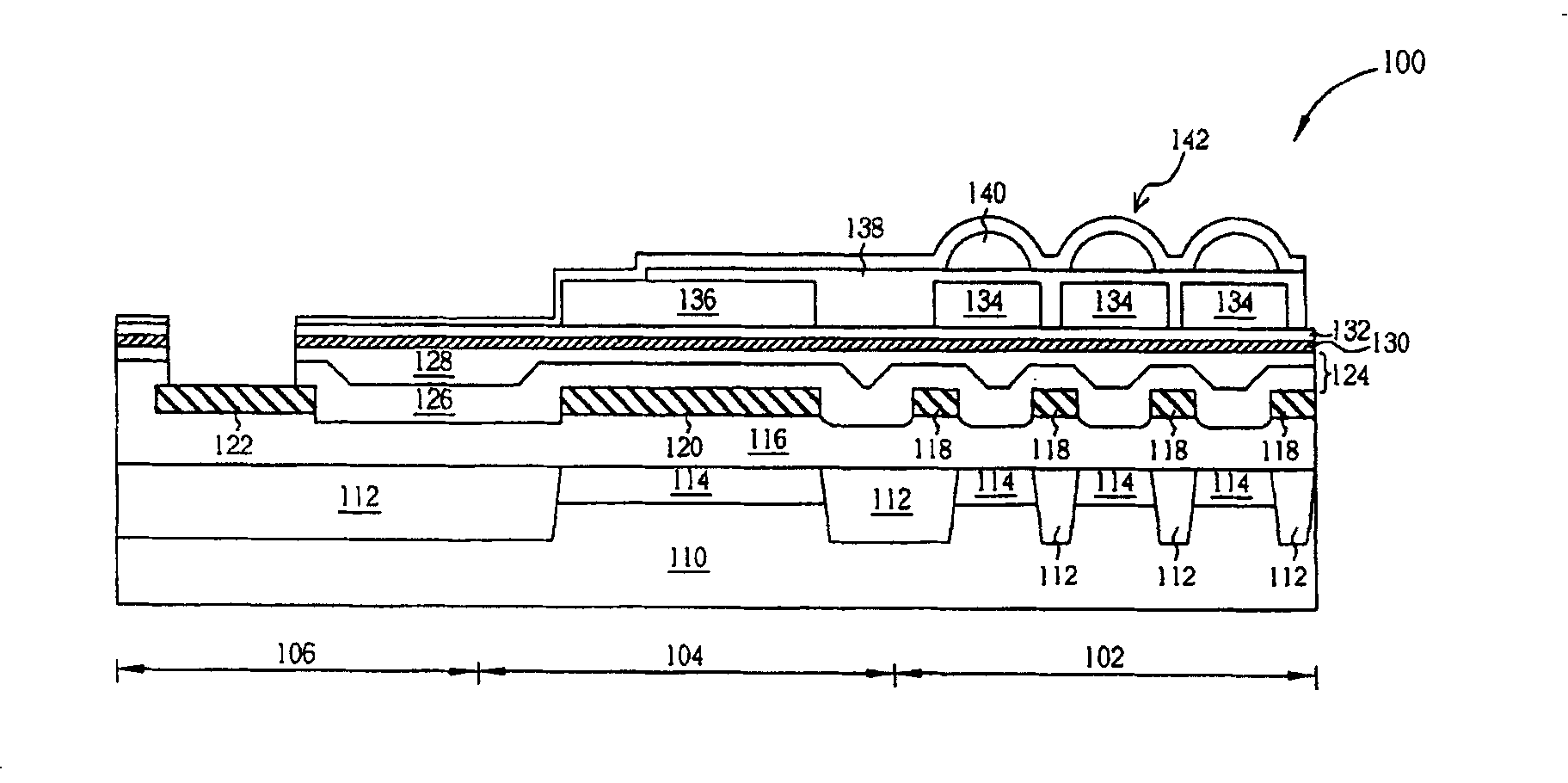
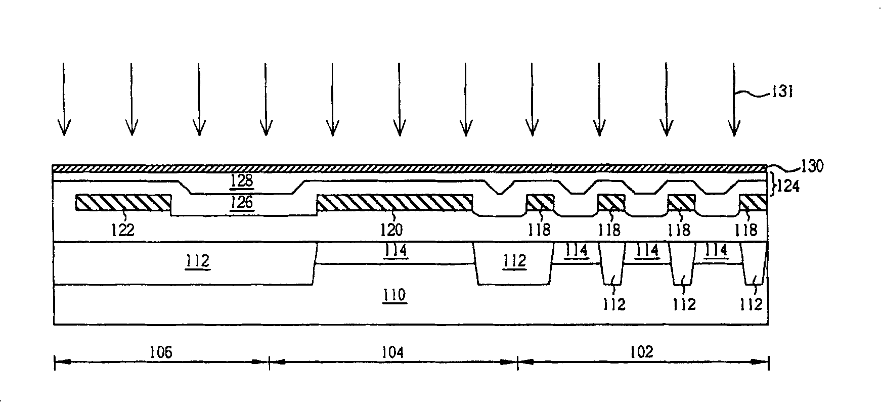
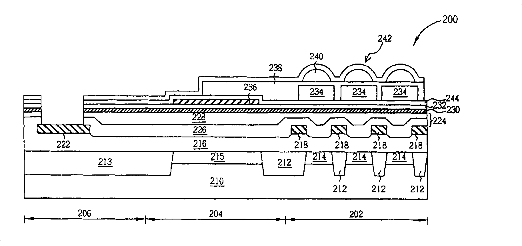
[0045] see image 3 , image 3An image sensing element 200 according to the present invention is shown. The image sensing device 200 includes a semiconductor substrate 210 , a pixel array area 202 , a logic area 206 , and an optical black area 204 . The pixel array area 202 is located on the semiconductor substrate 210 and includes a photo-sensing unit array 214 . The logic area 206 is located on the semiconductor substrate 210 and includes peripheral circuits. The optical black area 204 is located between the pixel array area 202 and the logic area 206 on the semiconductor substrate, including a photo-sensing unit 215 located on the semiconductor substrate 210, a first planarization layer 216 located on the photo-sensing unit 215, a The second planarization layer 224 is located on the first planarization layer 216 , and an optical black layer 236 is located on the second planarization layer 224 .

[0046] It should be noted that the optical black layer 236 includes a meta...


PUM


Abstract

The invention provides an image sensing element and a producing method. The method is characterized in that a flat layer is formed on a semiconductor base which comprises an pixel array area, an optical black area and a logical area to cover an optical sensing element array in the pixel array area and an optical element in the optical black area, then a patterned metal layer is formed in the area which corresponds to the pixel array area and the logical area on the flat layer, but the patterned metal layer can not be formed above the optical black area, a second flat layer is formed on the semiconductor base, and the second flat layer covers the patterned metal layer, an optical black layer is formed on the second flat layer of the optical black area under the condition that the temperature is below 400 DEG C. The method also includes steps for performing a dangling bond passivation technology on a photosensitive diode contained in the optical sensing elements of the pixel array area and the optical black area after the second flat layer is formed and before the optical black layer is formed.

Description

technical field [0001] The present invention relates to an image sensor and its manufacturing method, in particular to a complementary metal oxide semiconductor transistor image sensor and its manufacturing method. Background technique [0002] Complementary metal-oxide-semiconductor transistor image sensors (CMOS image sensors, CIS) and charge-coupled devices (charge-coupled devices, CCDs) are optical circuit components commonly used in the prior art to convert light into electronic signals. Both of them have a wide range of applications, including scanners, video cameras, and cameras, etc., but because charge-coupled devices are limited by the high price and large volume, currently the complementary metal-oxide-semiconductor transistor image sensor on the market Meters are more common. [0003] Since the complementary metal-oxide-semiconductor transistor image sensor is produced by traditional semiconductor technology, it can greatly reduce the required cost and component...

Claims


Application Information

Patent Timeline
Patent Type & Authority Patents(China)
IPC IPC(8): H01L21/822H01L27/146
Inventor 温增飞罗斯裘萨派鄢如心林家辉施俊吉黄建尧柯登渊彭念祖
Owner UNITED MICROELECTRONICS CORP
Why Eureka
Try Eureka