Transistor and image sensor

An image sensor and transistor technology, applied in semiconductor devices, electrical components, circuits, etc., can solve the problems of increasing dark current and affecting the performance of image sensors, and achieve the effect of suppressing the increase of dark current, reducing the effect of electric field enhancement, and improving performance

Active Publication Date: 2019-05-28
SHANGHAI INTEGRATED CIRCUIT RES & DEV CENT
View PDF3 Cites 0 Cited by
  • Summary
  • Abstract
  • Description
  • Claims
  • Application Information

AI Technical Summary

Problems solved by technology

Furthermore, the electrons generated by the strong electric field diffuse to the photodiode, increasing the dark current and affecting the performance of the image sensor

Method used


Image

  • Transistor and image sensor
  • Transistor and image sensor
  • Transistor and image sensor

Examples


Embodiment Construction

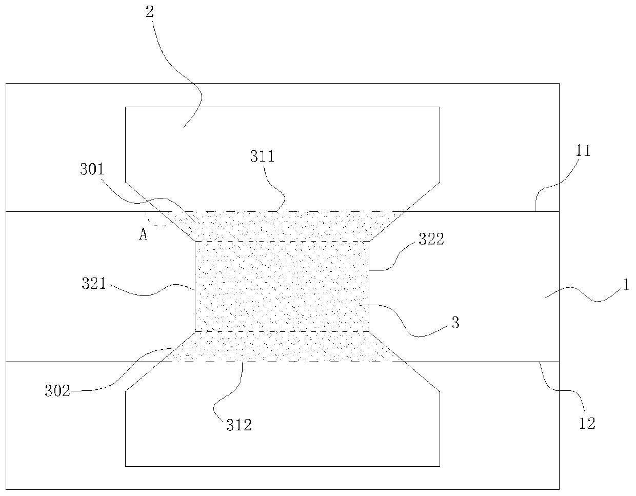
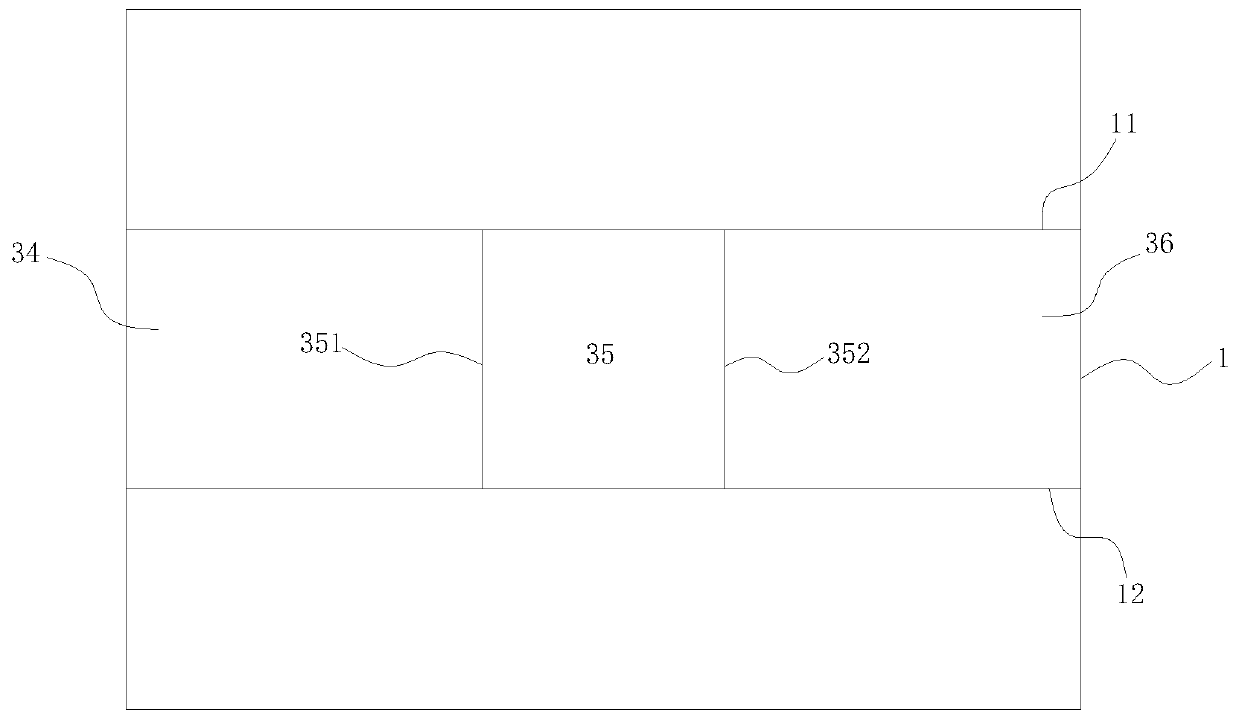
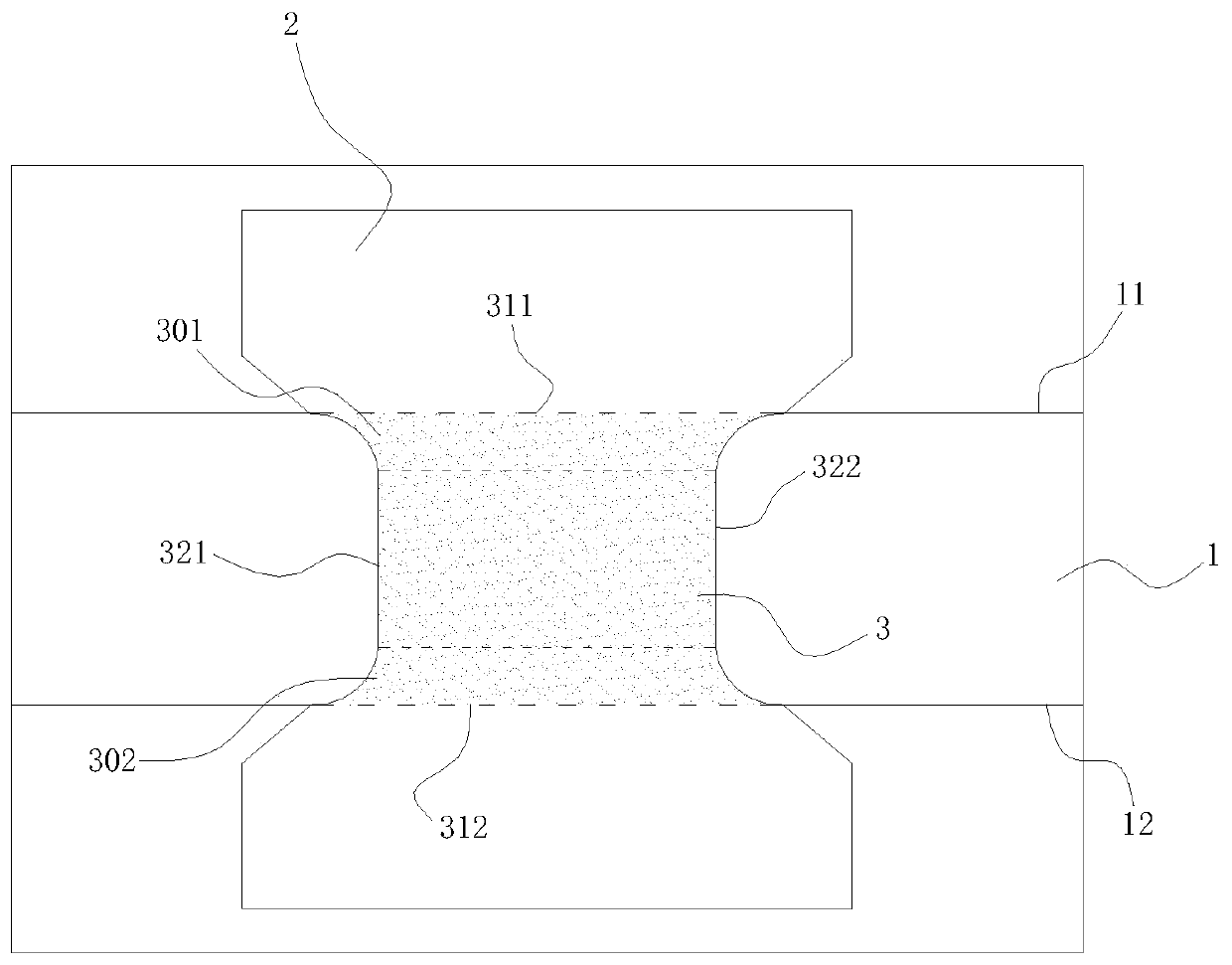
[0026] Example embodiments will now be described more fully with reference to the accompanying drawings. Example embodiments may, however, be embodied in many forms and should not be construed as limited to the embodiments set forth herein; rather, these embodiments are provided so that this disclosure will be thorough and complete, and will fully convey the concept of example embodiments to those skilled in the art. The same reference numerals denote the same or similar structures in the drawings, and thus their repeated descriptions will be omitted.

[0027] The described features, structures, or characteristics may be combined in any suitable manner in one or more embodiments. In the following description, numerous specific details are provided in order to give a thorough understanding of embodiments of the invention. However, those skilled in the art will appreciate that the technical solutions of the present invention may be practiced without one or more of the specific...


PUM


Abstract

The present invention discloses a transistor and an image sensor. The transistor comprises an active layer and a grid electrode, wherein the active layer comprises two side edges extending in a firstdirection; the grid electrode is arranged on the active layer, the projection of the grid electrode on the active layer and the edges of the two sides of the active layer form an overlapped region, and the overlapped region comprises two first side edges which are overlapped with the edges of the two sides of the active layer; and two second side edges respectively connected with the two first side edges; the overlapped region comprises two first regions adjacent to two side edges of the active layer, and in the first regions, the second side edges gradually extend in the direction far away from the overlapped region in the direction close to one side edge of the active layer adjacent to the first regions, respectively. The transistor can improve the dark current of the CMOS image sensor at low temperature.

Description

technical field [0001] The invention relates to the field of semiconductors, in particular to a transistor and an image sensor with the transistor. Background technique [0002] The basic unit in an image sensor is a pixel, and each pixel includes a photodiode and a MOS transistor. The photodiode is used to convert a light signal into a corresponding current signal, and the MOS transistor is used to transmit and read out the current signal converted by the photodiode. The source of the transfer transistor is connected to the photodiode, the silicon oxide layer is above the photodiode, and the PN photodiode forms an N-type doped region and a P-type doped region in sequence in a direction away from the substrate. Because the surface of PN photodiode is in direct contact with the silicon / silicon oxide section, there is a disadvantage of large dark current. Therefore, in the traditional image sensor, a surface clamping structure is introduced in the image sensor to reduce the da...

Claims


Application Information

Patent Timeline
Patent Type & Authority Applications(China)
IPC IPC(8): H01L29/06H01L29/78H01L27/146
Inventor 孙德明
Owner SHANGHAI INTEGRATED CIRCUIT RES & DEV CENT
Why Eureka
Try Eureka