Video sensing element and method for making the same

An image sensing element and light sensing technology, which is applied in the direction of electrical components, semiconductor/solid-state device manufacturing, radiation control devices, etc., can solve problems such as damage, and achieve the effects of reducing leakage current, improving dark current, and good performance

Inactive Publication Date: 2009-04-15
UNITED MICROELECTRONICS CORP
View PDF8 Cites 0 Cited by
  • Summary
  • Abstract
  • Description
  • Claims
  • Application Information

AI Technical Summary

Problems solved by technology

However, since the gate is formed before the protective layer is formed, there is still a risk of damage to the sensing area of ​​the photodiode during the formation of the gate using the plasma etching process

Method used


Image

  • Video sensing element and method for making the same
  • Video sensing element and method for making the same
  • Video sensing element and method for making the same

Examples


Embodiment Construction

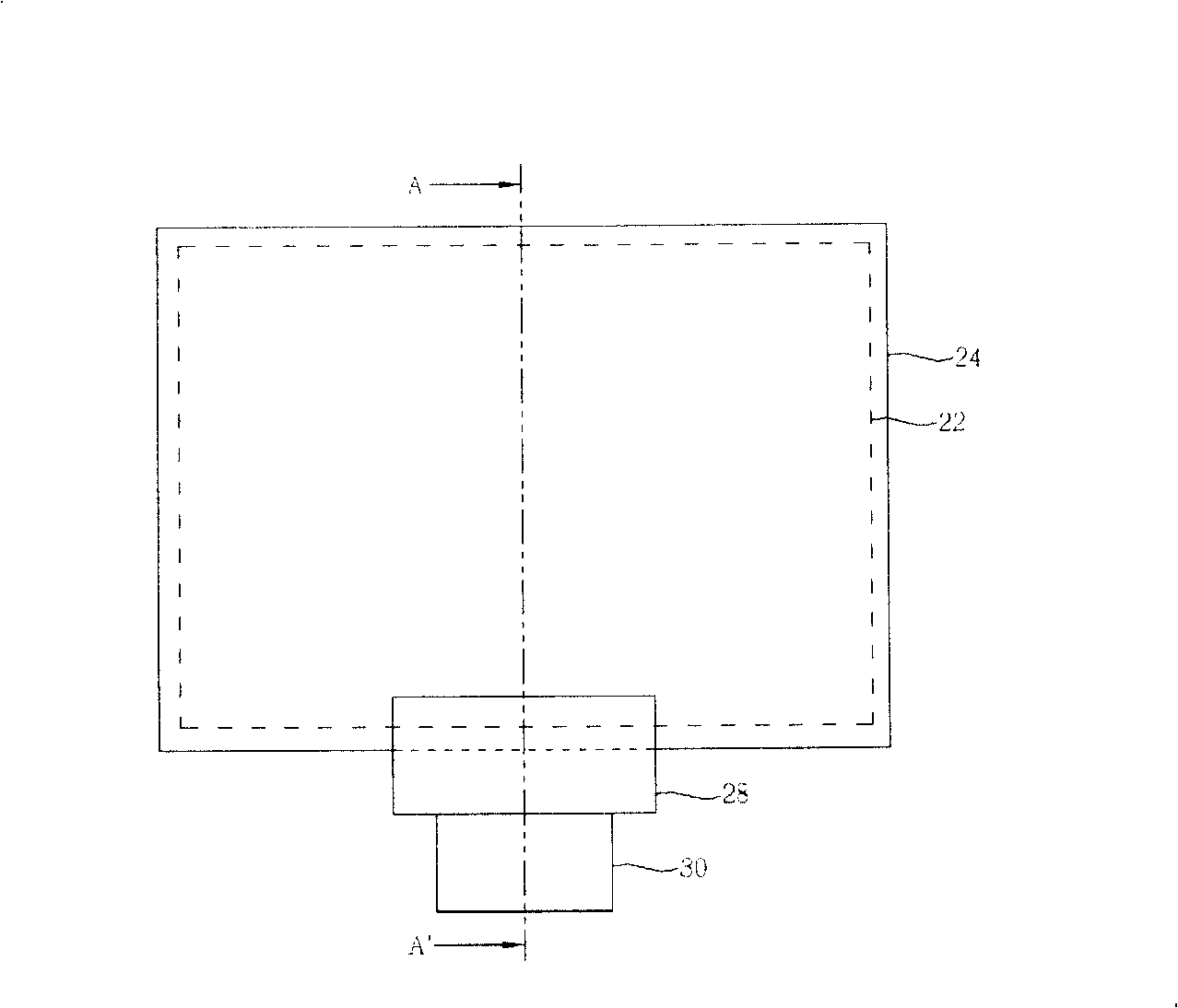
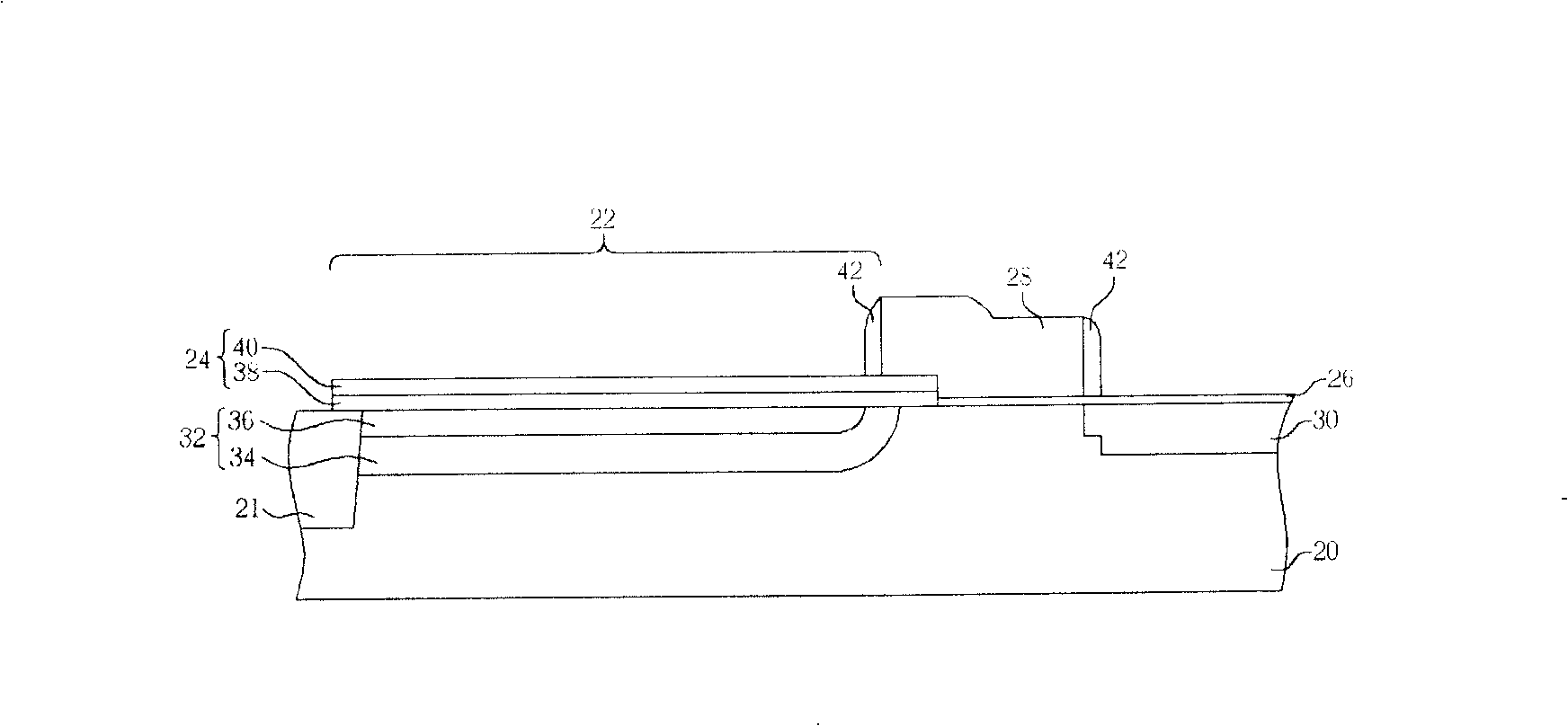
[0032] see figure 1 and 2 , figure 2 yes figure 1 Sectional view along line AA' in . The image sensing element according to the present invention can be a CMOS image sensing element, including a substrate 20, a photo-sensing region 22, a dielectric protection layer 24, a gate insulating layer 26, a gate 28, and a doped Miscellaneous area 30. The image sensing device is isolated from other devices by the shallow trench isolation structure 21 . The image sensing device according to the present invention is also suitable for isolation in other ways such as LOCOS.

[0033] The substrate 20 can be a p-type or n-type semiconductor substrate. The light sensing region 22 is located in the substrate 20 . The photosensitive region 22 may include a photosensitive layer 32 , which is a photosensitive material. For example, when the substrate 20 is a p-type substrate, the photosensitive layer 32 may include an n-type lightly doped layer 34 and a p-type heavily doped layer 36 . PIN...


PUM


Abstract

The invention relates to a preparing method of image sensing element, it mainly forming a dielectric protection layer on the light sensing area before forming the gate electrode of MOS, so during the course of forming MOS component, the surface damage of the light sensing area caused by plasma or etch can be avoided, so phenomenon of generating dark-current can be improved. The invention discloses image sensing element as this method, it characterized in that the gate electrode can cascade over the dielectric protection layer, at the same time because the surface of light sensing area is flat, it possesses perfect property.

Description

technical field [0001] The invention relates to an image sensor and its manufacturing method, in particular to a complementary metal oxide semiconductor transistor image sensor using a photosensitive diode and its manufacturing method. Background technique [0002] Complementary metal oxide semiconductor transistor image sensors (CMOS image sensors, CIS) and charge-coupled devices (charge-coupled devices, CCDs) are optical circuit components commonly used in the prior art to convert light into electronic signals. The application of the two The range is very wide, including scanners, video cameras, and cameras, etc. However, because the carrier coupling device is limited by the high price and large size, currently the complementary metal oxide semiconductor transistor image sensor is more popular in the market. Complementary metal-oxide-semiconductor transistor image sensors are manufactured by traditional semiconductor technology, so the required cost and component size can ...

Claims


Application Information

Patent Timeline
Patent Type & Authority Patents(China)
IPC IPC(8): H01L27/146H01L21/82
Inventor 高境鸿
Owner UNITED MICROELECTRONICS CORP
Why Eureka
Try Eureka