Pixel structure and preparation method of a stacked image sensor

An image sensor and pixel structure technology, applied in the field of image sensors, can solve the problems of deep junction depth and inability to achieve, and achieve the effect of good isolation effect, good dark current and less surface defects

Active Publication Date: 2021-01-29
SHANGHAI INTEGRATED CIRCUIT RES & DEV CENT +1
View PDF5 Cites 0 Cited by
  • Summary
  • Abstract
  • Description
  • Claims
  • Application Information

AI Technical Summary

Problems solved by technology

Due to the influence of the pre-process, it is usually impossible to achieve a deep junction depth, and it cannot have a good sensitivity to near-infrared or quantum efficiency.

Method used


Image

  • Pixel structure and preparation method of a stacked image sensor
  • Pixel structure and preparation method of a stacked image sensor
  • Pixel structure and preparation method of a stacked image sensor

Examples


Embodiment Construction

[0041] The specific embodiment of the present invention will be further described in detail below in conjunction with the accompanying drawings.

[0042] It should be noted that, in the following specific embodiments, when describing the embodiments of the present invention in detail, in order to clearly show the structure of the present invention for the convenience of description, the structures in the drawings are not drawn according to the general scale, and are drawn Partial magnification, deformation and simplification are included, therefore, it should be avoided to be interpreted as a limitation of the present invention.

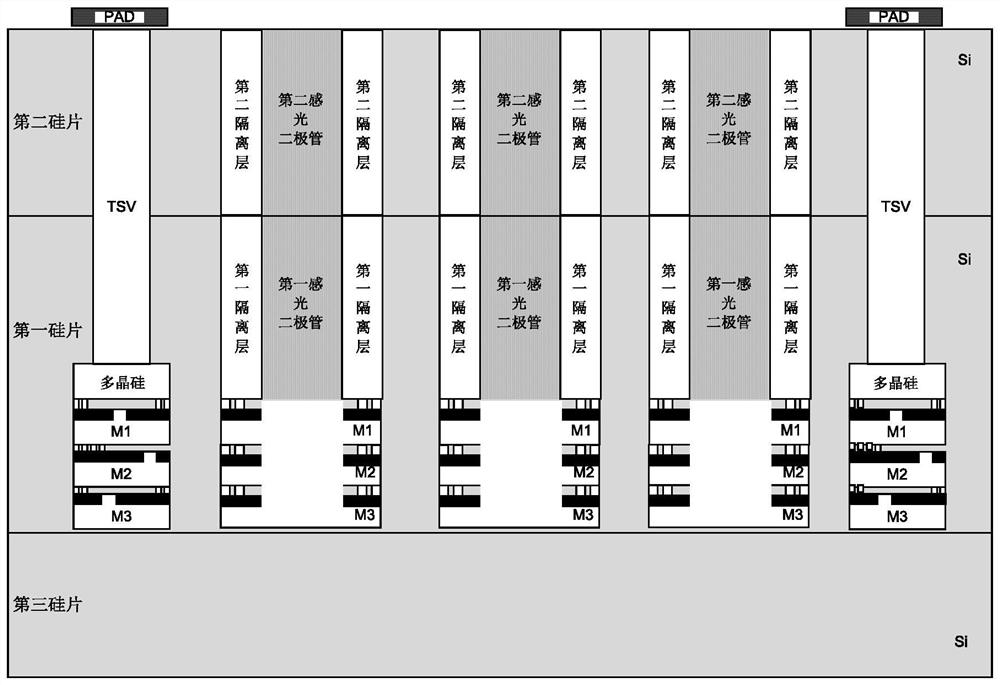
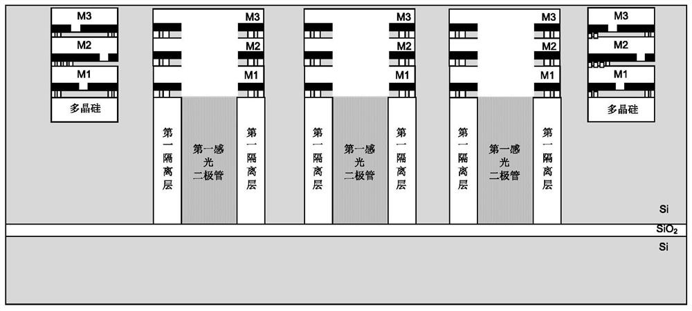
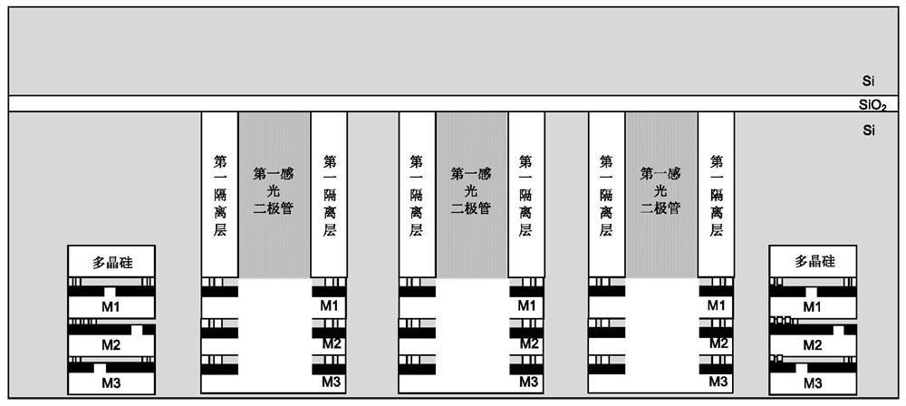
[0043] In the following specific embodiments of the present invention, please refer to figure 1 , figure 1 It is a schematic diagram of the pixel structure of a stacked image sensor according to a preferred embodiment of the present invention. Such as figure 1 As shown, a stacked image sensor pixel structure of the present invention is built on a ...


PUM

PropertyMeasurementUnit
widthaaaaaaaaaa
sizeaaaaaaaaaa

Abstract

The invention discloses a stacked mage sensor pixel structure and a fabrication method thereof. A first silicon wafer, a second silicon wafer and a third silicon wafer are vertically stacked by a bonding mode, wherein the first silicon wafer and the second silicon wafer are respectively formed from a remaining upper-layer thin bulk silicon substrate after a SiO2 layer and a lower-layer thick bulksilicon substrate of a standard SOI silicon wafer are stripped, a first light-sensitive diode array is arranged on the first silicon wafer, a second light-sensitive diode array is arranged on the second silicon wafer, a surface of each second light-sensitive diode is aligned and bonded with a surface of each corresponding first light-sensitive diode, so that the formed stacked image sensor chip has a junction which can be deepen to a SiO2 layer of the SOI silicon wafer, a dark current is better, the quantum efficiency can be effectively improved at a near-infrared band, the sensitivity is relatively high, a filling factor is relatively high, a very good comprehensive effect such as light-sensitive performance can be achieved for a small-size pixel element, the near-infrared quantum efficiency is compatible, and the small pixel size is also compatible.

Description

technical field [0001] The present invention relates to the technical field of image sensors, and more particularly, to a stacked near-infrared image sensor pixel structure and a preparation method thereof. Background technique [0002] Image sensors are an important part of digital cameras. According to the different components, it can be divided into two categories: CCD (Charge Coupled Device, charge-coupled device) and CMOS (Complementary Metal-Oxide Semiconductor, metal oxide semiconductor device). A prerequisite for the wide application of CMOS sensors is their higher sensitivity, shorter exposure time and shrinking pixel size. [0003] Among them, pixel sensitivity, one of the important performance indicators of CMOS image sensors, is mainly determined by the product of fill factor (the ratio of photosensitive area to the entire pixel area) and quantum efficiency (the number of electrons generated by photons bombarding the screen). In CMOS image sensors, in order to ...

Claims


Application Information

Patent Timeline
Patent Type & Authority Patents(China)
IPC IPC(8): H01L27/146
CPCH01L27/1461H01L27/1464H01L27/14652H01L27/14689
Inventor 李琛段杰斌
Owner SHANGHAI INTEGRATED CIRCUIT RES & DEV CENT
Why Eureka
Try Eureka