Silicon carbide-based gallium nitride micron wire array photoelectric detector and preparation method thereof

A photodetector, silicon carbide-based technology, applied in circuits, electrical components, semiconductor devices, etc., can solve the problems of slow development of micro-nano gallium nitride detectors, low device crystal quality, large body surface area, etc., to increase photoelectricity The effect of contact area, long detection range and simple device structure

Pending Publication Date: 2021-12-17
ZHEJIANG XINKE SEMICON CO LTD
View PDF0 Cites 0 Cited by
  • Summary
  • Abstract
  • Description
  • Claims
  • Application Information

AI Technical Summary

Problems solved by technology

[0004] In summary, due to the slow development of micro-nano gallium nitride detectors, the crystal quality of existing devices is low, and the body surface area is large, resulting in large size

Method used


Image

  • Silicon carbide-based gallium nitride micron wire array photoelectric detector and preparation method thereof
  • Silicon carbide-based gallium nitride micron wire array photoelectric detector and preparation method thereof
  • Silicon carbide-based gallium nitride micron wire array photoelectric detector and preparation method thereof

Examples


Embodiment 1

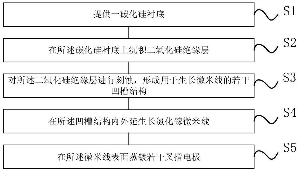
[0043] See figure 1 , figure 1 It is a silicon carbide-based gallium nitride micron line array photodetector provided by an embodiment of the present invention, including:

[0044] S1. Provide a silicon substrate. Specifically, the present embodiment adopts a 2-inch intrinsic type silicon wafer as a substrate, and the silicon substrate is a high-resistance silicon wafer (resistivity > 10 6 Ω·cm), the crystal orientation of the silicon wafer is .

[0045] S2. Deposit a silicon dioxide insulating layer on the silicon carbide substrate; in this embodiment, a 2.5-4 μm silicon dioxide insulating layer can be formed on the surface of a 2-inch silicon wafer by a thermal reduction method.

[0046] S3. Etching the silicon dioxide insulating layer to form several groove structures for growing micron wires, wherein the width of the groove structure is 8-12 μm, and the depth of the groove structure is 3.5 to 4.5 μm. The spacing between the groove structures is 8-10 μm;

[0047] Concre...

Embodiment 2

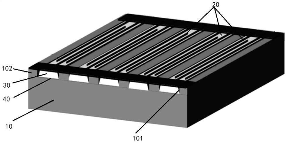
[0057] See Figure 2-Figure 6 , the silicon carbide-based gallium nitride micron line array photodetector of this embodiment can be prepared by the method of embodiment 1, and the device includes:

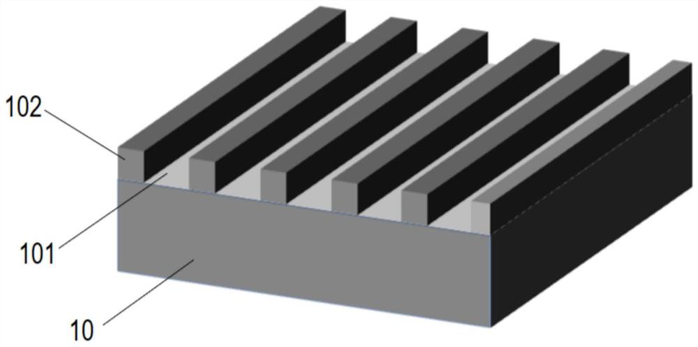
[0058] silicon carbide substrate 10;

[0059] A silicon dioxide insulating layer 102 is formed at intervals on the silicon carbide substrate 10, so that several groove structures 101 are formed on the substrate not covered with the silicon dioxide insulating layer 102, wherein the resistivity of the insulating layer 102 is greater than 10 16 Ω cm;

[0060] Gallium nitride micro-wires 30 are formed in the groove structure 101, and the extension direction of the gallium nitride micro-wires 30 is consistent with the extending direction of the groove structure 101, wherein there are multiple gallium nitride micro-wires 30 in the form of array shape;

[0061] The aluminum nitride buffer layer 40 is formed inside the gallium nitride micro-wire 30 of the groove structure 101; the alum...


PUM

PropertyMeasurementUnit
widthaaaaaaaaaa
depthaaaaaaaaaa
heightaaaaaaaaaa

Abstract

The invention discloses a silicon carbide-based gallium nitride micron wire array photoelectric detector and a preparation method thereof. The detector comprises: a silicon carbide substrate; silicon dioxide insulating layers formed on the silicon carbide substrate at intervals, so that a plurality of groove structures are formed on the substrate which is not covered with the silicon dioxide insulating layers; gallium nitride micron wires formed in the groove structures, wherein the extension direction of the micron wire is consistent with the extension direction of the groove structure; aluminum nitride buffer layers formed below the gallium nitride micron wires of the groove structures; and a plurality of interdigital electrodes arranged above the gallium nitride micron wires and the silicon dioxide insulating layer and parallel to the direction of the groove structures. According to the invention, the photoelectric detector has the good characteristics of high light/dark current, quick response, high on/off current ratio, wide detection range and the like, and the device structure is easy to grow and manufacture.

Description

technical field [0001] The invention belongs to the field of semiconductors, and in particular relates to a silicon carbide-based gallium nitride micron line array photodetector and a preparation method. Background technique [0002] Photodetectors work by converting light signals into electrical signals. Photodetectors are widely used in various fields of military and national economy. In the visible or near-infrared band, it is mainly used for ray measurement and detection, industrial automatic control, photometry, etc.; in the infrared band, it is mainly used for missile guidance, infrared thermal imaging, infrared remote sensing, etc. Compared with the first and second generation semiconductor materials, gallium nitride (GaN) has a wider bandgap (band gap of 3.4eV, radiation resistance, high temperature resistance, low dielectric constant and other excellent properties, and has been widely used and Electronic power devices and optoelectronic devices. With the rapid dev...

Claims


Application Information

Patent Timeline
Patent Type & Authority Applications(China)
IPC IPC(8): H01L31/0352H01L31/0304H01L31/0224H01L31/102H01L31/18
CPCH01L31/0352H01L31/03044H01L31/022408H01L31/102H01L31/1856Y02P70/50
Inventor 李京波孙一鸣王小周
Owner ZHEJIANG XINKE SEMICON CO LTD
Why Eureka
Try Eureka