Repair circuitry and method for preventing electrical fuse from being burned during static discharge testing

A technique for electrostatic discharge testing and repairing circuits, applied to circuits, electrical components, static memory, etc., to achieve the effect of avoiding programming

Active Publication Date: 2008-03-05
TAIWAN SEMICON MFG CO LTD
View PDF0 Cites 6 Cited by
  • Summary
  • Abstract
  • Description
  • Claims
  • Application Information

AI Technical Summary

Problems solved by technology

Even though the Vq pad has the ESD clamp 101, som...

Method used


Image

  • Repair circuitry and method for preventing electrical fuse from being burned during static discharge testing
  • Repair circuitry and method for preventing electrical fuse from being burned during static discharge testing
  • Repair circuitry and method for preventing electrical fuse from being burned during static discharge testing

Examples


Embodiment Construction

[0038] Since e-fuse is widely used in integrated circuits, a robust e-fuse circuit can effectively improve the overall SoC yield. In a generalized embodiment, the present invention provides an improved repair circuit for storing IP cores having at least one switching device and at least one control circuit to prevent e-fuse from being deliberately programmed, thereby improving overall SoC yield.

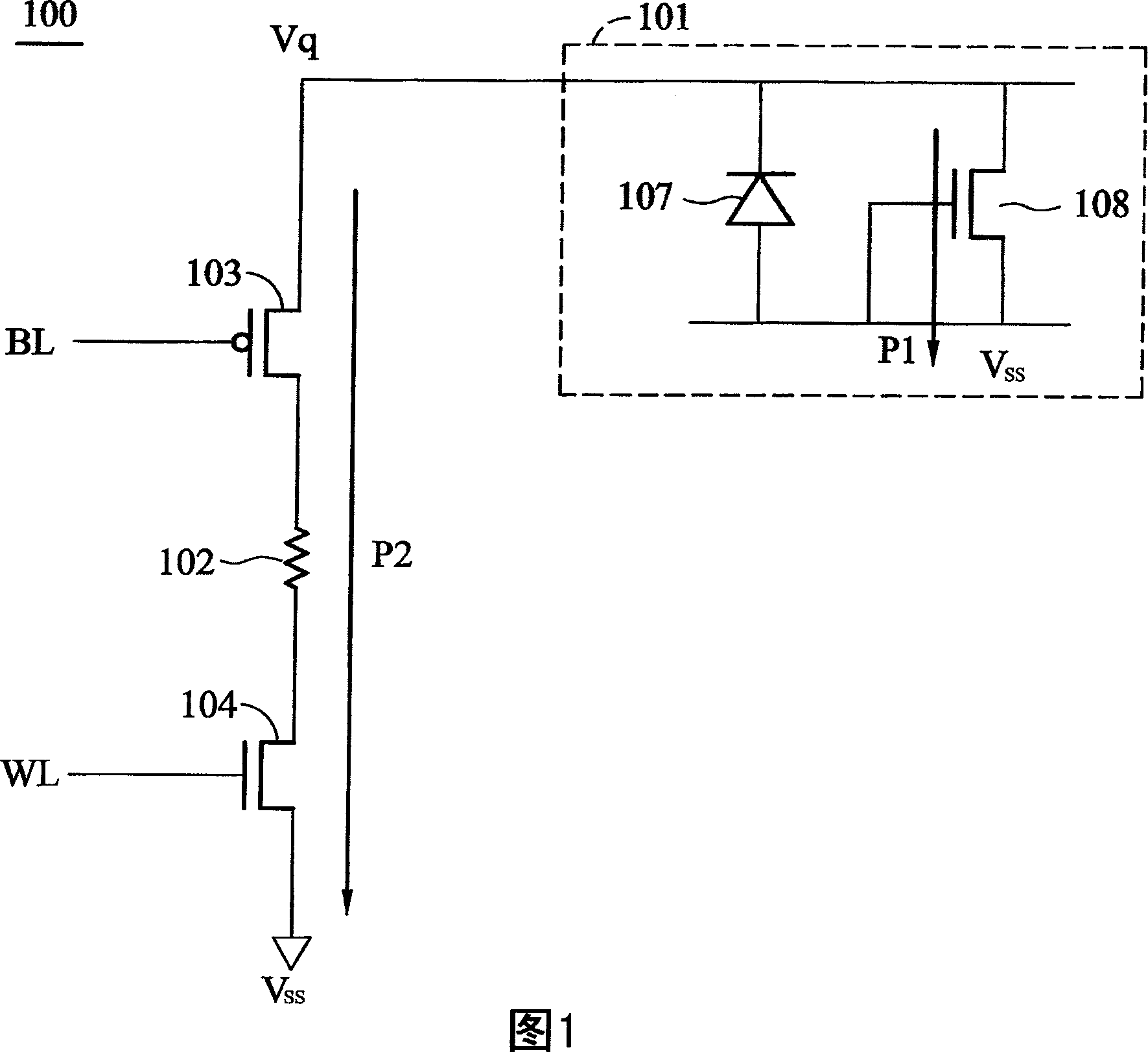
[0039] Figure 1 has been described and discussed in the Background of the Invention. No further discussion is required here.

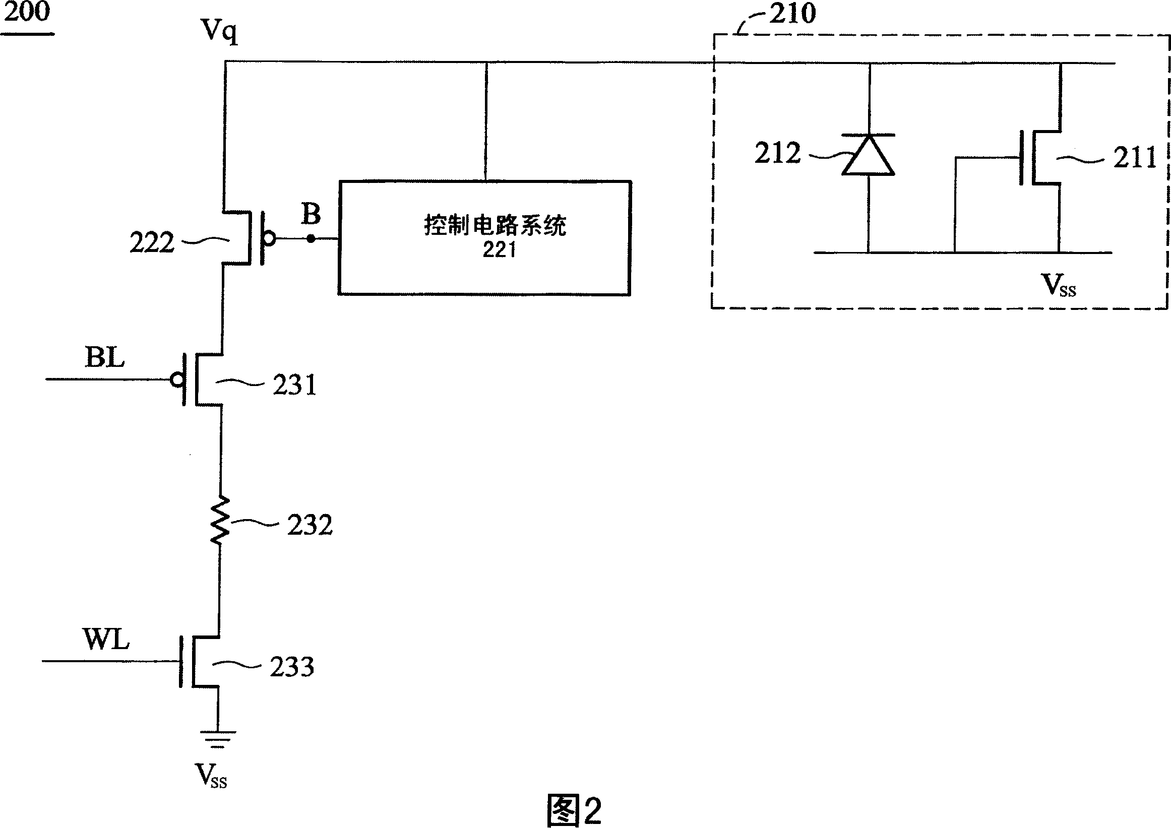
[0040]Figure 2 shows a repair circuit 200 with improved ESD protection in accordance with a preferred embodiment of the present invention. In addition to the ESD clamping circuit 210 including two diodes 211 and 212 , the improved repairing circuit 200 also includes a switching device 222 and a control circuit system (or referred to as a control circuit) 221 .

[0041] In FIG. 2, the embodiment has at least one electronic fuse 232 forming at least one condu...


PUM


Abstract

The present invention provides a method of repairing a circuit and preventing electronic fuses from burning out during an electrostatic discharge test, the repairing circuit consists of at least one pad forming a partial conduction path between a positive voltage supply (Vq) and a lower voltage supply source (Vss) The electronic fuse constitutes. The repair circuit includes at least one switch device and at least one control circuit. The at least one switching device has a control terminal and is coupled between the Vq pad and the at least one electronic fuse. The at least one control circuit is respectively coupled to the control terminal and the Vq pad. When a positive high voltage is applied to the Vq pad, the control circuit delays the conduction state of the switching device for a predetermined period of time, so as to block the stray current generated when ESD occurs. Therefore, the repair circuit prevents the at least one electronic fuse from being incorrectly programmed.

Description

technical field [0001] The present invention relates generally to repair circuits for semiconductor devices, and more particularly to repair circuits with electrostatic discharge (ESD) protection against accidental blowing of electronic fuses due to ESD. Background technique [0002] A system-on-chip (SoC, System-on-Chip) usually embeds a storage IP core with a large number of integrated bits in each SoC. Because the memory IP core is of high cell density, the embedded memory is more susceptible than any other element on the chip to defects that already exist on the silicon substrate. Thus, new self-healing algorithms have been developed to test and repair memory devices on SoCs. This new technology can increase typical SoC yields by as much as 80 percent compared to traditional external test and repair systems [0003] The self-healing principle is usually implemented by adding an electronic fuse circuit on the semiconductor device, such as chip ID (chip ID), serial numbe...

Claims


Application Information

Patent Timeline
IPC IPC(8): G11C29/44G11C17/16G11C17/18H01L27/02
CPCG11C29/02G11C29/027G11C17/18
Inventor 蔡铭宪廖宏仁林松杰
Owner TAIWAN SEMICON MFG CO LTD
Why Eureka
Try Eureka