Chip welding quality checking method

A technology for chip welding and testing methods, which is applied in the direction of measuring electricity, measuring devices, measuring electrical variables, etc., can solve the problems of inaccurate positioning of welding quality problems, long development cycle of test programs, etc., to achieve rapid reuse and improve detection efficiency. Effect

Inactive Publication Date: 2008-03-19
NANJING ZHONGXING XIN SOFTWARE CO LTD
View PDF0 Cites 10 Cited by
  • Summary
  • Abstract
  • Description
  • Claims
  • Application Information

AI Technical Summary

Problems solved by technology

However, the premise of using the online detection method is that the electronic device to be tested can run the test program, so there are solder joints that cannot be detected by the test program
In addition, the test program development cycle is long, and the location of welding quality problems is not accurate

Method used


Image

  • Chip welding quality checking method
  • Chip welding quality checking method

Examples


Embodiment Construction

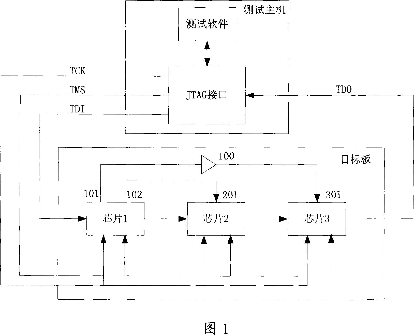
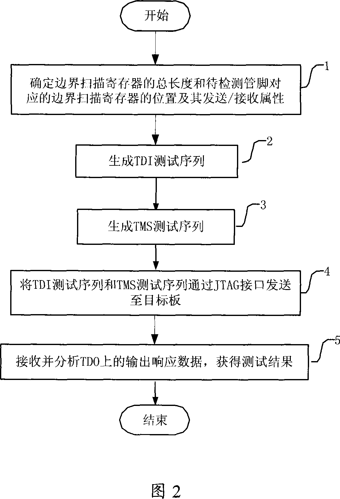
[0023] The key points of the technical scheme of the present invention are: generate a specific test data packet containing a TDI test sequence and a corresponding TMS test sequence according to the position information of the JTAG shift register corresponding to the solder joint to be detected in the PCB board, and test the The data packet is sent to the device to be tested through the JTAG interface, and the welding quality is accurately detected by analyzing the output response of the device to be tested.

[0024] The present invention will be described in detail below in conjunction with the accompanying drawings.

[0025] FIG. 1 is a schematic diagram of the system structure of the detection method for chip soldering quality of the present invention. As shown in Figure 1, the test software is run on the test host, and the test host is connected to the target board (PCB board) to be tested which contains 3 chips with JTAG ports through the JTAG interface. At the same time...


PUM


Abstract

The present invention provides a chip welding quality testing method, and includes the following procedures: the total length of the boundary scanning register and the position of the boundary scanning register corresponding to the tube feet to be tested can be determined according to a BSDL document and the number of the tube feet to be tested; and a TDI testing sequence containing the tube foot testing data can be generated, wherein, each digit of the tube foot testing data corresponds to a value of the boundary scanning register in a JTAG chain to be tested, and the length is the total length of the boundary scanning register. A TMS testing sequence can be generated according to the above TDI testing sequence. The TDI testing sequence and the TMS testing sequence can be sent to a target board when the JTAG is in the Shift-DR state. The tube output responding date on the TDO can be analyzed, and the welding mistake can be judged when the shift register values of the receiving tube feet to be tested and the sending tube feet corresponding to the receiving tube feet are different.

Description

technical field [0001] The invention relates to a method for detecting soldering quality of a PCB (Printed Circuit Board, printed circuit board), in particular to a method for detecting soldering quality of chip pins in a PCB. Background technique [0002] In the process of soldering the chip to the PCB, due to problems such as soldering materials and soldering processes, soldering errors such as virtual soldering and bridging may occur, resulting in open or short circuits in electronic equipment. [0003] Existing detection methods for soldering quality of chip pins include off-line detection methods and on-line detection methods. Off-line detection methods include X-ray detection methods and the like. The X-ray detection method mainly uses X-ray equipment to emit X-rays to the electronic equipment after welding, and judges whether there is a problem with the solder joints by observing the reflection of the X-rays. This detection method is relatively intuitive, and the po...

Claims


Application Information

Patent Timeline
Patent Type & Authority Applications(China)
IPC IPC(8): G01R31/02
Inventor 秦永兵苏泽峰
Owner NANJING ZHONGXING XIN SOFTWARE CO LTD
Why Eureka
Try Eureka