Photoetching system mask proximity effect correction method

A technology of proximity effect and lithography system, which is applied in optics, originals for photomechanical processing, instruments, etc., can solve the problems of graphic couplets and strong phase shift mask technology that cannot be applied, so as to improve graphic fidelity, The effect of precision control and imaging contrast enhancement

Inactive Publication Date: 2011-03-23
INST OF ELECTRICAL ENG CHINESE ACAD OF SCI
View PDF0 Cites 0 Cited by
  • Summary
  • Abstract
  • Description
  • Claims
  • Application Information

AI Technical Summary

Problems solved by technology

[0011] The technical problem to be solved in the present invention is: to overcome the deficiencies of mask layout in some IC designs, such as the graphic couplets and strong phase shift mask technology caused by the simultaneous presence of X and Y graphics, which cannot be applied, and propose a mask graphic Proximity effect correction method, the invention improves the fidelity of graphic imaging by adding phase-shifting proximity effect, especially the mask of 65nm and below nodes in the ArF lithography system

Method used


Image

  • Photoetching system mask proximity effect correction method
  • Photoetching system mask proximity effect correction method
  • Photoetching system mask proximity effect correction method

Examples


Embodiment Construction

[0029] The present invention will be further described below in conjunction with the accompanying drawings and specific embodiments.

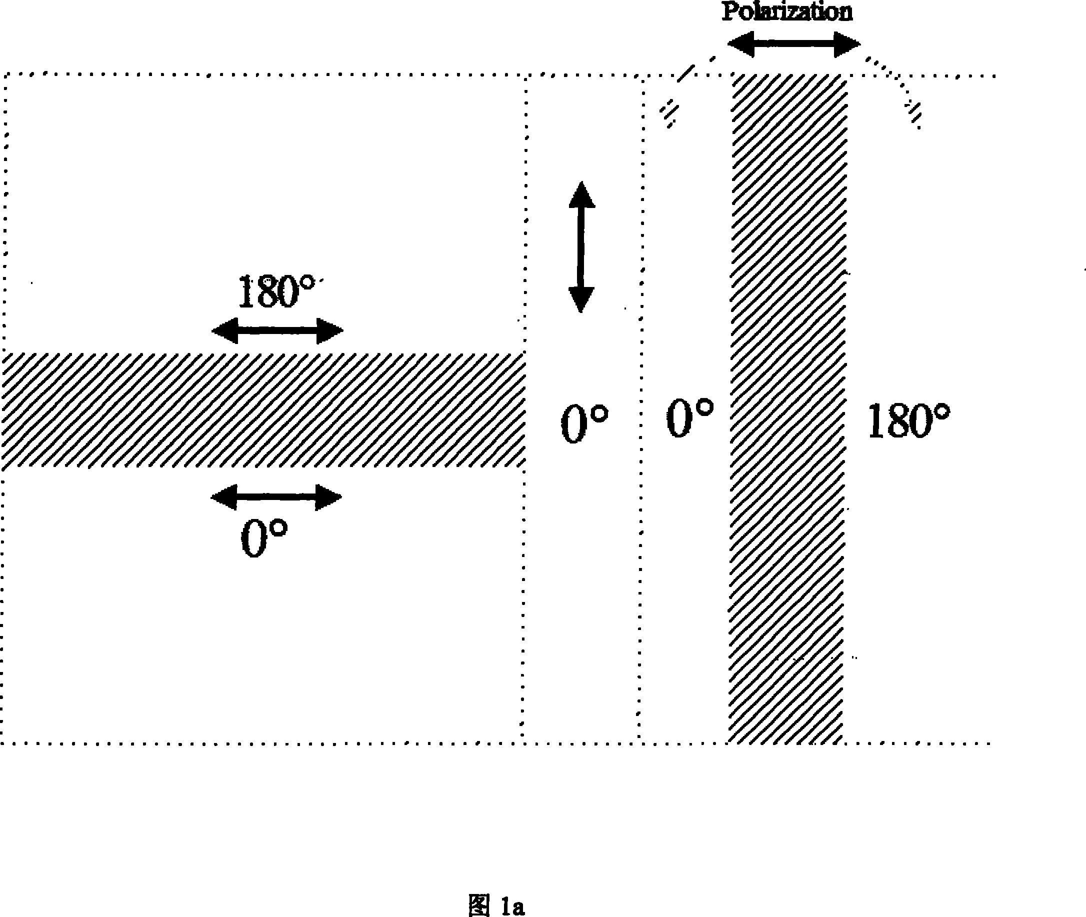
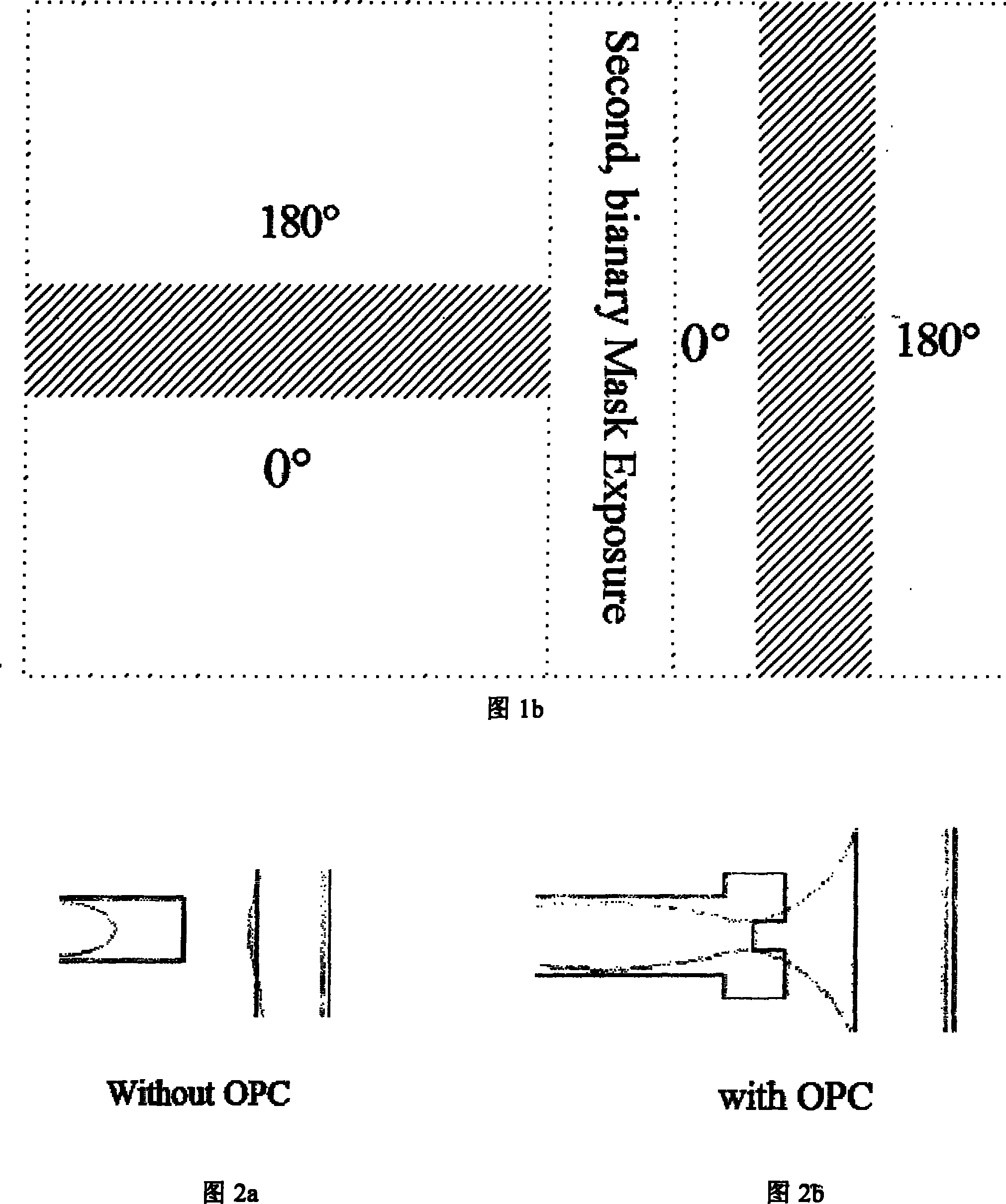
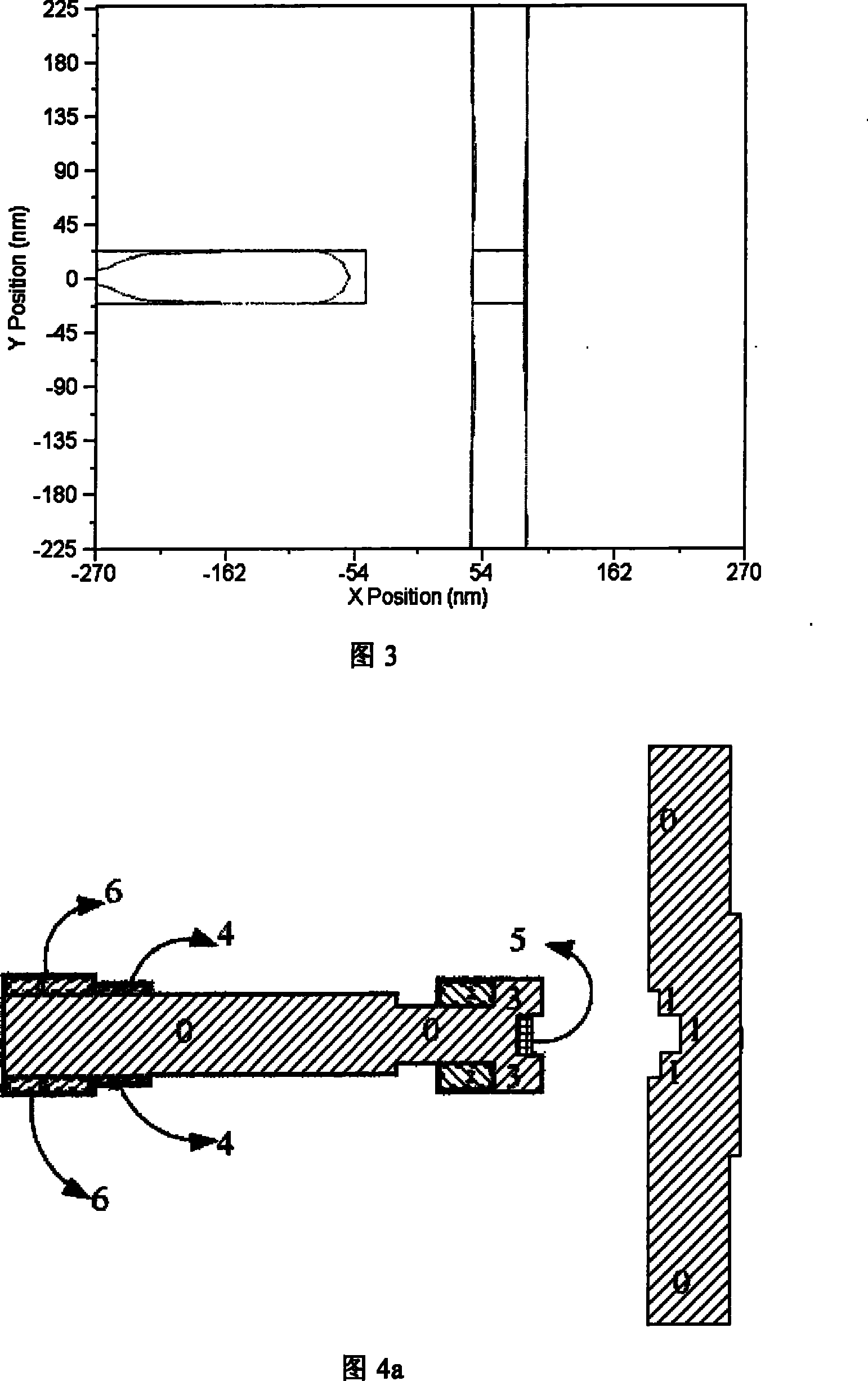
[0030] The specific operation steps of the correction method of the present invention are: first according to image 3 As shown in the original mask photolithography simulation exposure graphics results, it is judged that the part of the distortion that needs to be corrected by proximity effect; according to the position of the distorted graphics, at the corresponding position of the mask graphics, the proximity effect correction method is used to correct the mask graphics. Pre-segmentation and addition: At the junction of X and Y graphics, initially add serifs according to the method of phase-shift proximity effect correction, and add proximity effect correction with a certain transmittance and 180-degree phase shift on both sides of the serif Split graphics, preset as Figure 4a The phase-shift proximity effect correction shown, the size of ...


PUM


Abstract

The present invention relates to a correction method for lithography system mask proximity effect; first of all, the final graphic on a silicon chip can be compared with the design graphic of the mask to find out the distorted places, according to the position of the distorted graphic, using the correction method of proximity effect, and at the corresponding position on the mask graphic, the maskgraphic can be pre-segmented and added in the way that a lining line is added at the joint of X and Y trend graphics, and proximity-effect correction segmented graphics which are nontransparent, and has 180 degrees phase offset are added on the two sides of the lining line, and together forms an initial framework of the phase-offset proximity-effect correction; then the exposure result after adding the phase-offset proximity-effect correction can be observed through lithography simulation method, and according to the exposure result, errors between the exposure result and expected graphic canbe measured by the simulation software; and according to the errors, the related parameters, such as size and transmission of the phase-offset proximity-effect correction on the mask plate can be adjusted until the errors between the final developing graphic on the silicon chip and the original mask design graphic is less than minus or plus 10 percent, the allowed deviation Limit of industry lithography error.

Description

technical field [0001] The invention relates to a mask proximity effect correction method for a photolithography system, in particular to a mask proximity effect correction method for 65nm and below nodes in an ArF photolithography system. Background technique [0002] The resolution of optical lithography is gradually improving. With the gradual reduction of lithographic feature size, the proximity effect is more obvious. However, the traditional proximity effect correction has insufficient correction accuracy or cannot meet the requirements in some graphic structure applications. . Taking the T-shaped graph structure as an example, the X-direction graph has obvious line-end shortening effect, and the traditional proximity effect correction method cannot meet the requirements in terms of correction accuracy and spatial size, and a new proximity effect correction method is urgently needed. [0003] At present, in order to improve the imaging resolution of similar patterns s...

Claims


Application Information

Patent Timeline
Patent Type & Authority Patents(China)
IPC IPC(8): G03F1/14G03F1/36
Inventor 高松波李艳秋
Owner INST OF ELECTRICAL ENG CHINESE ACAD OF SCI
Why Eureka
Try Eureka