Photoetching system mask proximity effect correction method

A technology of proximity effect and lithography system, applied in optics, originals for photomechanical processing, instruments, etc., can solve the problems of graphic couplets and strong phase shift mask technology, and achieve improved graphic fidelity, Save time and process cost, the effect of precision control

Inactive Publication Date: 2008-03-19
INST OF ELECTRICAL ENG CHINESE ACAD OF SCI
View PDF0 Cites 21 Cited by
  • Summary
  • Abstract
  • Description
  • Claims
  • Application Information

AI Technical Summary

Problems solved by technology

[0011] The technical problem to be solved in the present invention is: to overcome the deficiencies of mask layout in some IC designs, such as the graphic couplets and strong phase shift mask technology caused by the simultaneous presence of X and Y graphics, which cannot be applied, and propose a mask graphic Proximity effect correction method, the invention improves the fidelity of graphic imaging by adding phase-shifting proximity effect, especially the mask of 65nm and below nodes in the ArF lithography system

Method used


Image

  • Photoetching system mask proximity effect correction method
  • Photoetching system mask proximity effect correction method
  • Photoetching system mask proximity effect correction method

Examples


Embodiment Construction

[0029] The present invention will be further described below in conjunction with the accompanying drawings and specific embodiments.

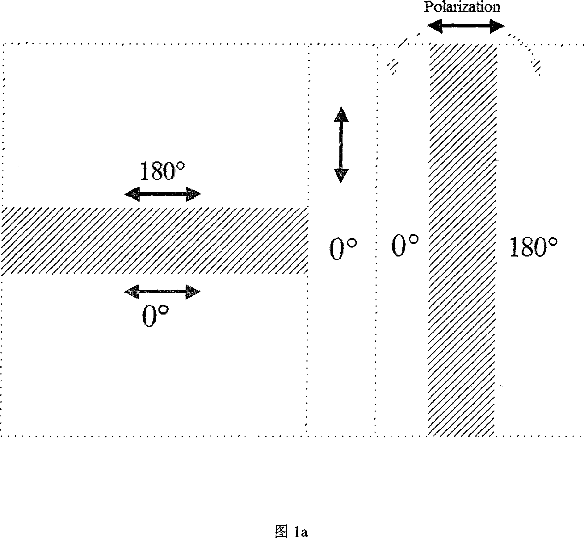
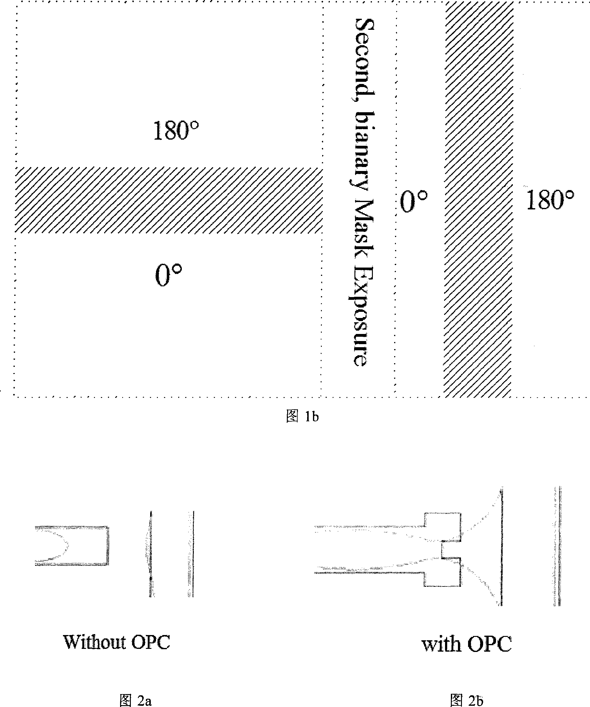
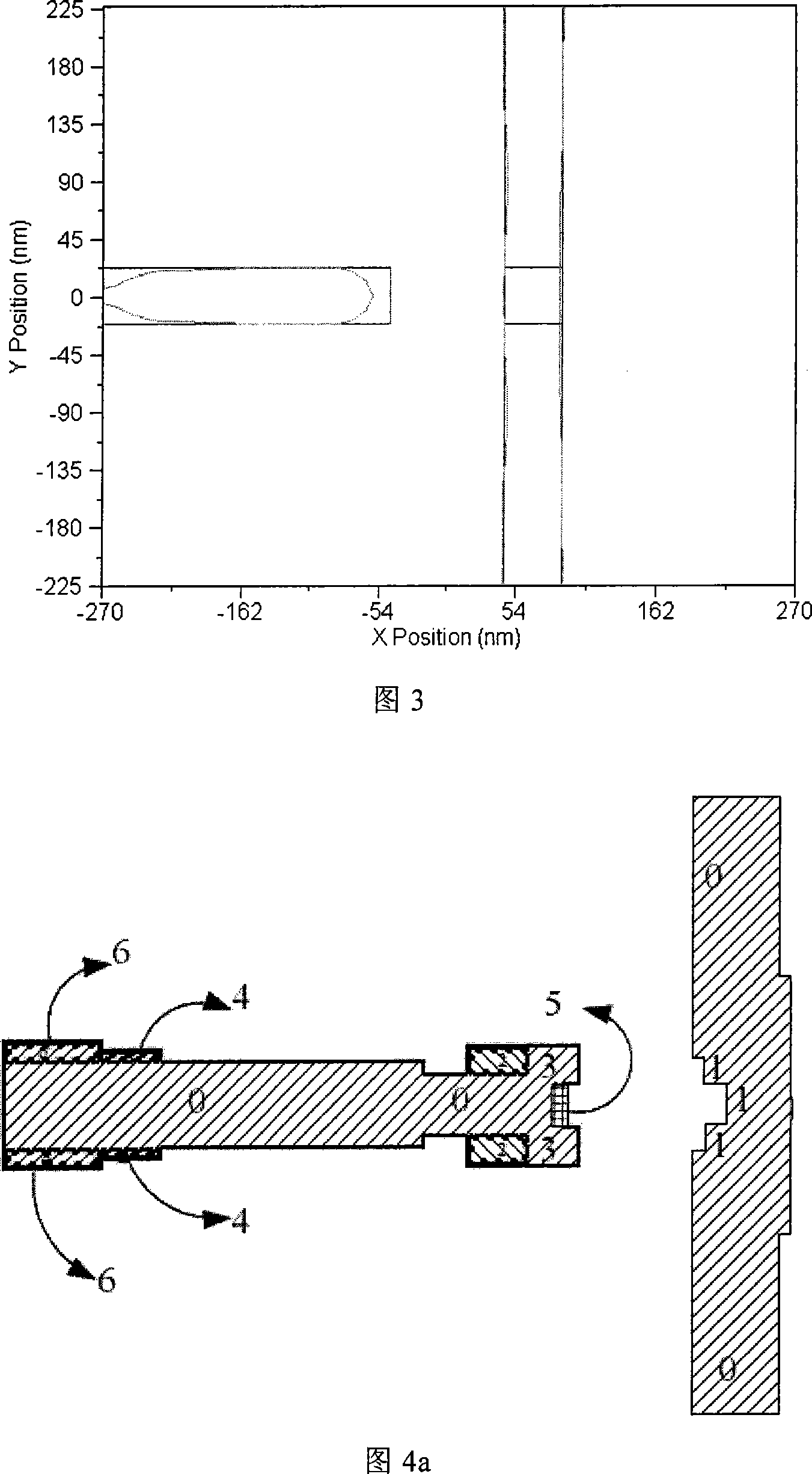
[0030] The specific operation steps of the correction method of the present invention are as follows: firstly, according to the graphic result after the original mask lithography simulation exposure shown in Fig. The corresponding position of the mask pattern is pre-segmented and added using the proximity effect correction method: at the joint of the X and Y directions, serifs are preliminarily added according to the method of phase-shift proximity effect correction, and the serifs are added on both sides. Proximity effect correction split pattern with a certain transmittance and 180-degree phase shift is pre-set as phase-shifted proximity effect correction as shown in Figure 4a. The size of each split pattern is based on the exposure result shown in Figure 3 and the original mask pattern. The degree of distortion is set, and then re-exposure is ...


PUM


Abstract

A mask proximity effect correction method for a lithography system. First, find out the distortion of the final pattern on the silicon wafer compared with the mask design pattern, and correct it according to the proximity effect at the corresponding position of the mask pattern according to the position of the distorted pattern. The method to pre-segment and add the mask graphics: add serifs at the junction of X and Y graphics, and add non-transparent proximity effect correction graphics with 180-degree phase shift on both sides of the serifs, together Constitute the preliminary framework of phase-shift proximity effect correction; then observe the exposure result after adding phase-shift proximity effect correction through lithography simulation method, and according to the exposure result, use simulation software to measure the error between the exposure result and the expected pattern, according to This error adjusts the size, transmittance and other related parameters of the phase-shift proximity effect correction on the reticle until the error between the developed pattern on the silicon wafer and the original design pattern of the reticle is less than the allowable limit of ±10% deviation in industrial lithography .

Description

technical field [0001] The invention relates to a mask proximity effect correction method for a photolithography system, in particular to a mask proximity effect correction method for 65nm and below nodes in an ArF photolithography system. Background technique [0002] The resolution of optical lithography is gradually improving. With the gradual reduction of lithographic feature size, the proximity effect is more obvious. However, the traditional proximity effect correction has insufficient correction accuracy or cannot meet the requirements in some graphic structure applications. . Taking the T-shaped graph structure as an example, the X-direction graph has obvious line-end shortening effect, and the traditional proximity effect correction method cannot meet the requirements in terms of correction accuracy and spatial size, and a new proximity effect correction method is urgently needed. [0003] At present, in order to improve the imaging resolution of similar patterns s...

Claims


Application Information

Patent Timeline
Patent Type & Authority Applications(China)
IPC IPC(8): G03F1/14G03F1/36
Inventor 高松波李艳秋
Owner INST OF ELECTRICAL ENG CHINESE ACAD OF SCI
Why Eureka
Try Eureka