Print circuit board before-typesetting processing system and method

A printed circuit board and processing system technology, applied in the direction of electrical digital data processing, special data processing applications, instruments, etc., can solve the problems of wasting substrate materials, wasting production costs of board factories, and expensive board costs, achieving low production costs, The effect of high work efficiency

Inactive Publication Date: 2008-03-19
INVENTEC CORP
View PDF0 Cites 10 Cited by
  • Summary
  • Abstract
  • Description
  • Claims
  • Application Information

AI Technical Summary

Problems solved by technology

[0003] However, the above-mentioned calculation procedure of the waste value of the substrate board by manual calculation is prone to inevitable human error, so if the value of the waste material of each circuit board unit corresponding to the substrate of different sizes is not correctly calculated , the substrate size corresponding to the least value of wasted material cannot be correctly selected, and the substrate mat

Method used


Image

  • Print circuit board before-typesetting processing system and method
  • Print circuit board before-typesetting processing system and method

Examples


Embodiment Construction

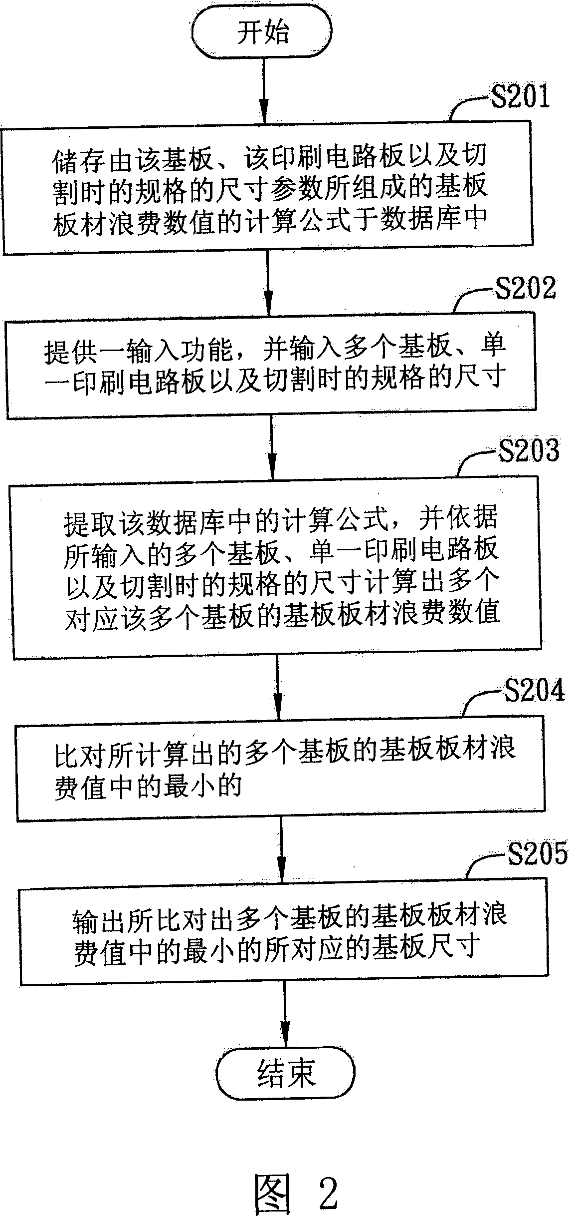
[0028] The implementation of the present invention is described below through specific specific examples, and those skilled in the art can easily understand other advantages and effects of the present invention from the content disclosed in this specification. The present invention can also be implemented or applied through other different specific embodiments, and various modifications and changes can be made to the details in this specification based on different viewpoints and applications without departing from the spirit of the present invention.

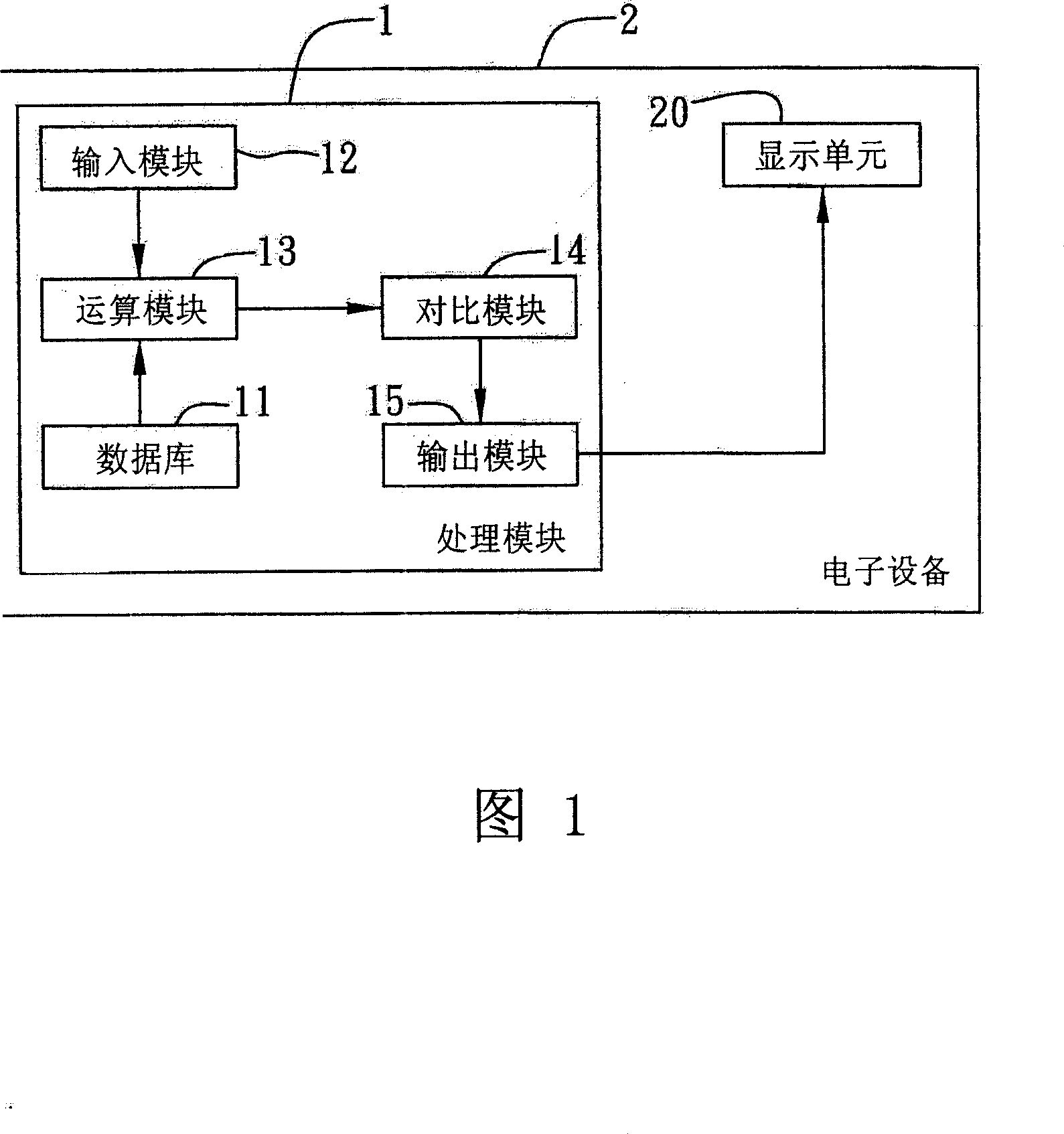
[0029] As shown in FIG. 1 , it is a schematic block diagram of the basic structure of an embodiment of a processing system 1 before layout of printed circuit boards according to the present invention. The processing system 1 before the layout of the printed circuit board is applied to the layout program for planning the position to be cut of the printed circuit board (PCB) on the substrate, wherein the layout program is common k...


PUM


Abstract

The present invention relates to a system and a method of a printing circuit wafer before a typesetting. First, a database storing a computational formula for calculating out the waste value of the baseplate stuffs is established. After the sizes of multiple baseplates, a single printing circuit wafer and the specifications in cutting are inputted through an input module, the waste values of the corresponding baseplate stuffs are worked out through a calculating module based on the computational formula as well as the input sizes of multiple baseplates, the single printing circuit wafer and the specifications in cutting, and finally the minimum value of the waste values of the multiple baseplate stuffs is found out through a contrasting module, and then the size of the baseplate, which is corresponding to the minimum value of the waste values of the multiple baseplate stuffs obtained by the contrasting module, is outputted through an output module to carry out a typesetting program, thereby reducing the manufacturing cost of a typesetting and improving the work efficiency as well.

Description

technical field [0001] The present invention relates to a processing system and method before typesetting of printed circuit boards, and more particularly, relates to a printed circuit board before the typesetting process used to plan the position to be cut of printed circuit board (PCB) on the substrate Processing system and method before typesetting. Background technique [0002] At present, the typesetting of printed circuit board (PCB) board factories is mainly based on manual calculation, that is, according to the size of the circuit board unit provided by the customer, the material wasted by each circuit board unit corresponding to the substrate of different sizes is manually calculated value, and then to determine what size substrate to choose, and then typesetting it. [0003] However, the above-mentioned calculation procedure of calculating the waste value of the substrate board by manual calculation is prone to inevitable human error, so if the value of the waste ...

Claims


Application Information

Patent Timeline
IPC IPC(8): G06F17/50
Inventor 胡莲于影杨淑敏
Owner INVENTEC CORP
Why Eureka
Try Eureka