Supercharge Your Innovation With Domain-Expert AI Agents!

Semiconductor device and method of manufacturing the same

A manufacturing method and semiconductor technology, applied in semiconductor/solid-state device manufacturing, semiconductor devices, semiconductor/solid-state device components, etc., can solve problems such as inner lead bounce

Inactive Publication Date: 2008-03-19
RENESAS TECH CORP
View PDF2 Cites 2 Cited by
  • Summary
  • Abstract
  • Description
  • Claims
  • Application Information

AI Technical Summary

Problems solved by technology

[0007] In addition, in paragraph [0022] of the above-mentioned Patent Document 2, it is disclosed that there is a problem that the tip of the inner lead bounces up due to the crushing process.

Method used


Image

  • Semiconductor device and method of manufacturing the same
  • Semiconductor device and method of manufacturing the same
  • Semiconductor device and method of manufacturing the same

Examples


Embodiment Construction

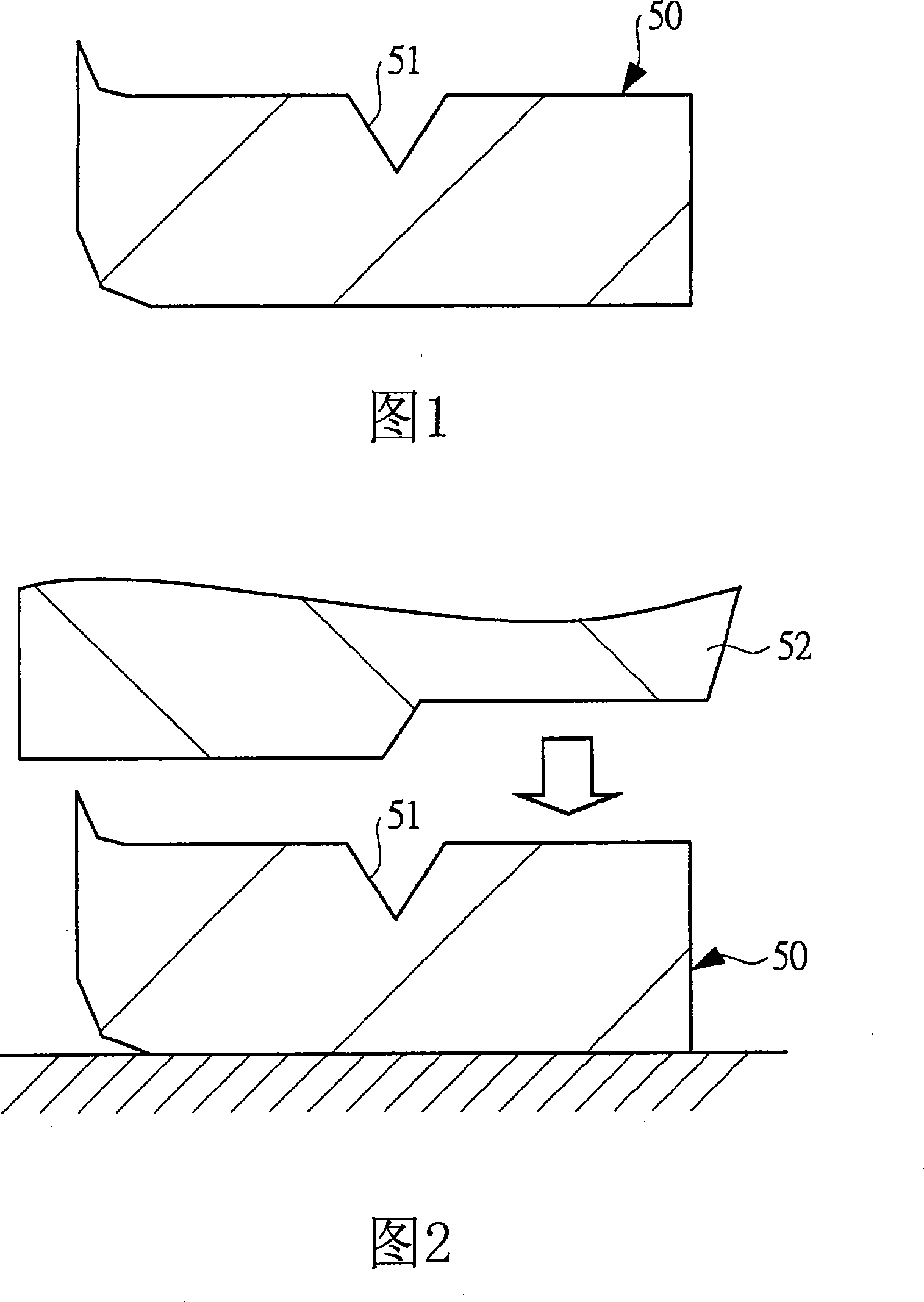
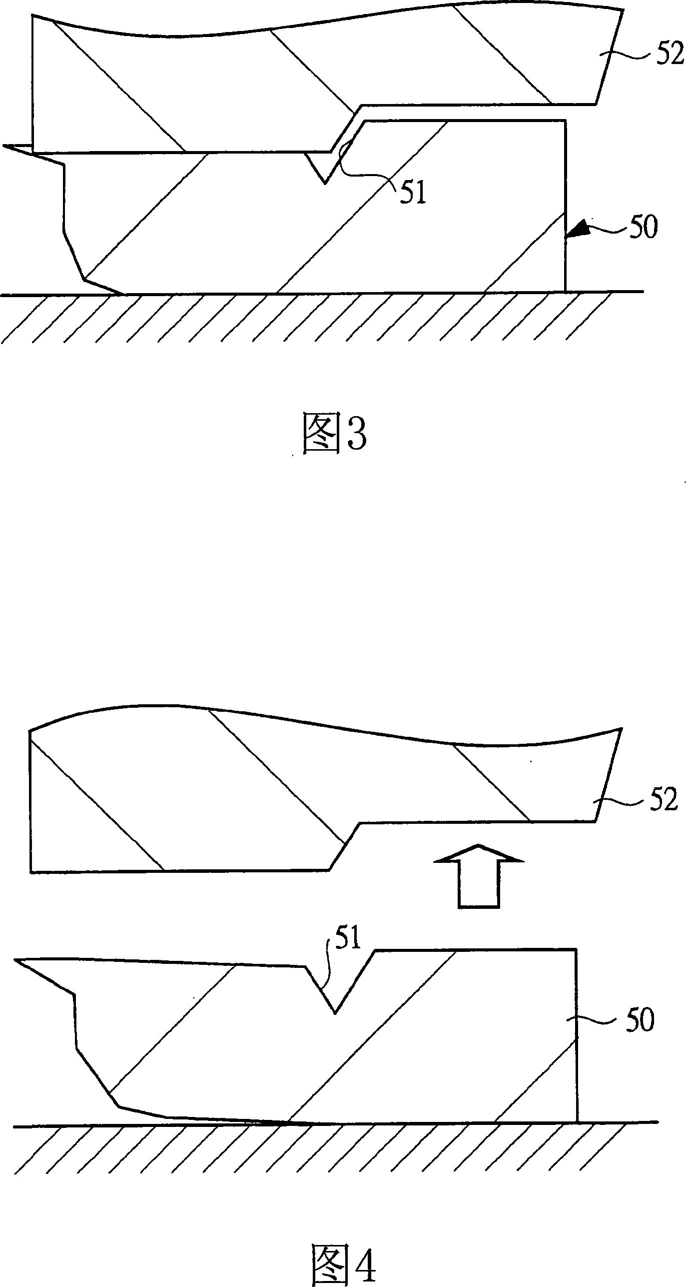
[0078] For the convenience of description, the following embodiments are divided into multiple parts or embodiments for description, but unless otherwise specified, the multiple parts or embodiments are not independent of each other, but there are modifications in which one part is the other part or all of them , detailed description, supplementary description, etc. Moreover, in the following embodiments, the number of elements (including number, value, amount, range, etc.) is not limited to the specific number, but may be above or below a specified number. In addition, in the following embodiments, the constituent elements (including element steps, etc.) can be regarded as unnecessary unless otherwise specified or clearly recognized as essential in principle. Similarly, in the following embodiments, when referring to the shape, positional relationship, etc. of components, etc., it may include substantially similar or similar shapes, etc., unless otherwise specified or in pri...


PUM


Abstract

In this invention, it is possible to improve the semiconductor device manufacturing yield. In a leadless package type semiconductor device manufacturing process, there is used a press frame wherein a front end portion each lead is subjected to a coining work. A semiconductor chip-side front end portion of the lead is inclined so as to become lower gradually toward the semiconductor chip. As a result, the amount of depression of the lead front end portion can be made small and hence it is possible to suppress or prevent spring-up of the lead front end portion. Further, the lead front end portion is formed obliquely and the amount of depression thereof is set larger than the thickness of a plating layer formed on the lead front end portion. As a result, when lead frames after formation of the plating layer are conveyed or stored stackedly, it is possible to diminish or prevent the occurrence of an inconvenience such that an overlying lead comes into contact with the plating layer of an underlying lead and causes a frictional scratch to be formed on the plating layer.

Description

technical field [0001] The present invention relates to a method of manufacturing a semiconductor device and a technology of a semiconductor device, and particularly relates to an effective technology applicable to a method of manufacturing a semiconductor device and a semiconductor device in which a wire-bonding portion with leads is crushed The so-called pressure frame. Background technique [0002] In leadless package type semiconductor devices represented by QFN (Quad Flat Non-leaded package, four-sided non-leaded flat package), in consideration of ensuring the bonding reliability of leads and bonding wires, sometimes a press frame is used for bonding in leads. The parts with welding lines are crushed (pressed). [0003] In addition, in leadless packaged semiconductor devices, the leads may fall off after the molding process due to the short lead wires. Therefore, in order to strengthen the adhesion between the leads and the molding resin, a portion of the surface of th...

Claims


Application Information

Patent Timeline
Patent Type & Authority Applications(China)
IPC IPC(8): H01L21/50H01L21/60H01L23/488H01L23/495
CPCH01L21/4842H01L24/48H01L2924/01023H01L23/3121H01L24/45H01L2924/01082H01L2224/48599H01L2924/01047H01L2924/01004H01L2924/01079H01L2224/85385H01L2224/48465H01L2924/01002H01L2224/48247H01L2924/14H01L23/49548H01L2924/01005H01L2924/01033H01L2924/01006H01L24/49H01L23/49582H01L2924/01029H01L2924/01078H01L2924/01014H01L2224/45144H01L2224/48091H01L2224/85439H01L2224/49171H01L2924/181H01L2224/48639H01L2224/05554H01L2924/00014H01L2924/00H01L23/48
Inventor 田中茂树长谷部一
Owner RENESAS TECH CORP
Features
  • R&D
  • Intellectual Property
  • Life Sciences
  • Materials
  • Tech Scout
  • Unparalleled Data Quality
  • Higher Quality Content
  • 60% Fewer Hallucinations
Learn More