Liquid crystal display panel and method for producing same
A technology for liquid crystal display panels and manufacturing methods, applied in nonlinear optics, instruments, optics, etc., capable of solving problems such as light leakage of liquid crystal display panels, maintaining the contrast of liquid crystal display panels, and partial blackness, so as to achieve the effect of avoiding light leakage or partial blackness
- Summary
- Abstract
- Description
- Claims
- Application Information
AI Technical Summary
Problems solved by technology
Method used
Image

Examples
no. 1 example
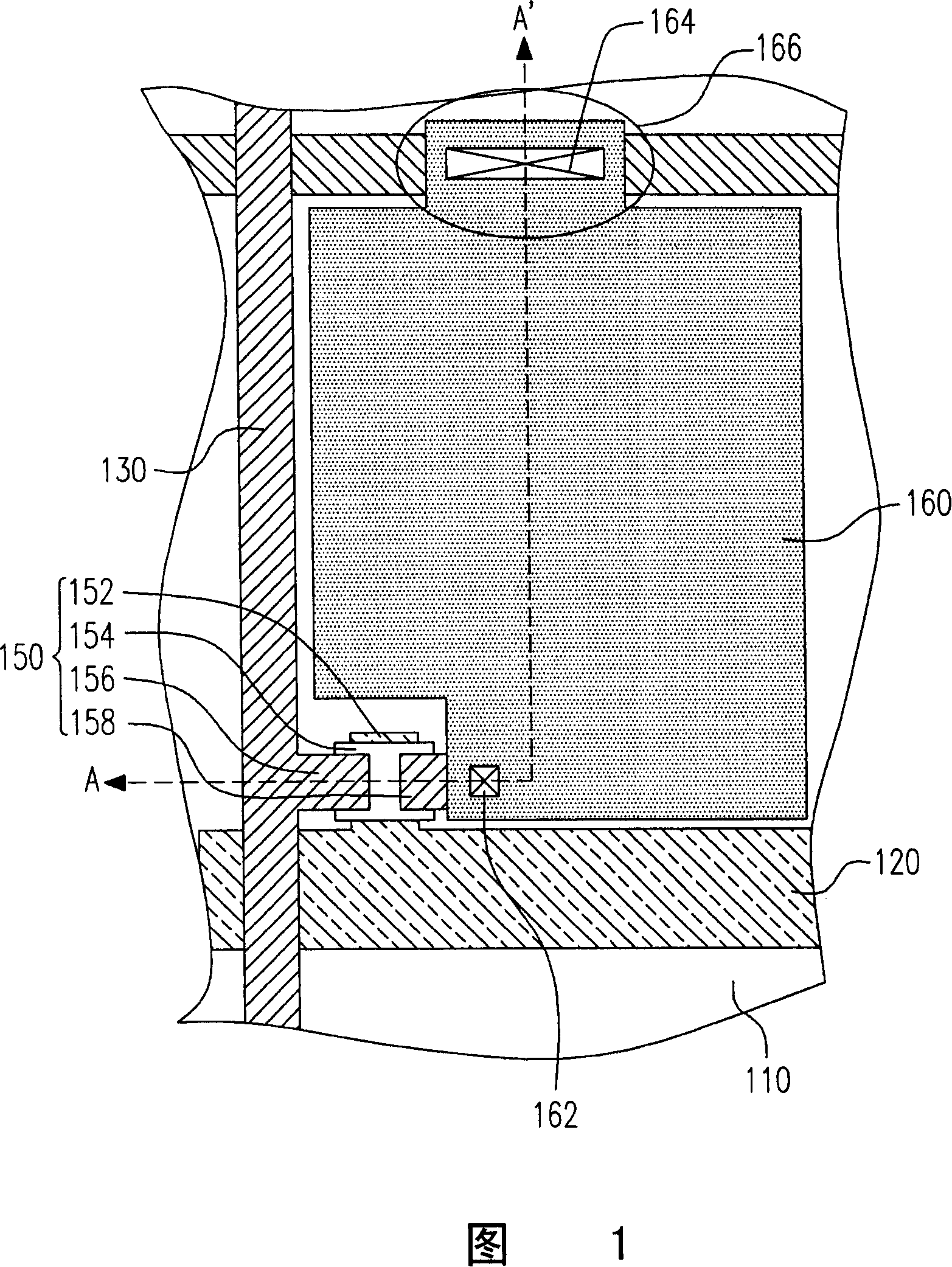
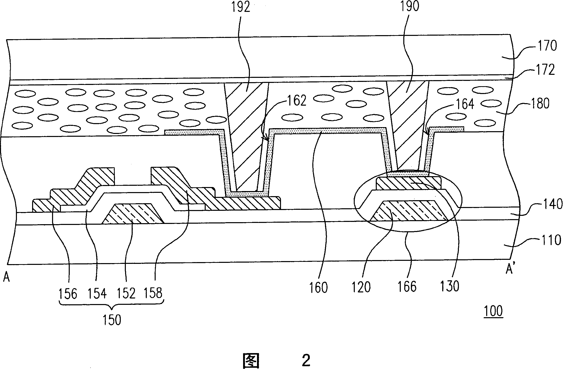
[0049] 3 is a schematic top view of one of the pixel structures of the thin film transistor array substrate of the liquid crystal display panel according to the first embodiment of the present invention, and FIG. 4 is a cross-sectional view of a liquid crystal display panel according to a preferred embodiment of the present invention, which is FIG. 3 Sectional view corresponding to BB' and CC'. Please refer to FIG. 3 and FIG. 4 together. The manufacturing method of the liquid crystal display panel 200 includes the following steps. Firstly, a first substrate 210 is provided, on which the thin film transistor manufacturing process is performed, wherein a plurality of gates 222 (only one is shown in the figure) and electrodes electrically connected to the gates 222 are formed on the substrate 210 A plurality of scanning lines 230 (only one is shown in the figure) are formed by, for example, first depositing a film layer and then performing an exposure process, a development proce...
no. 2 example
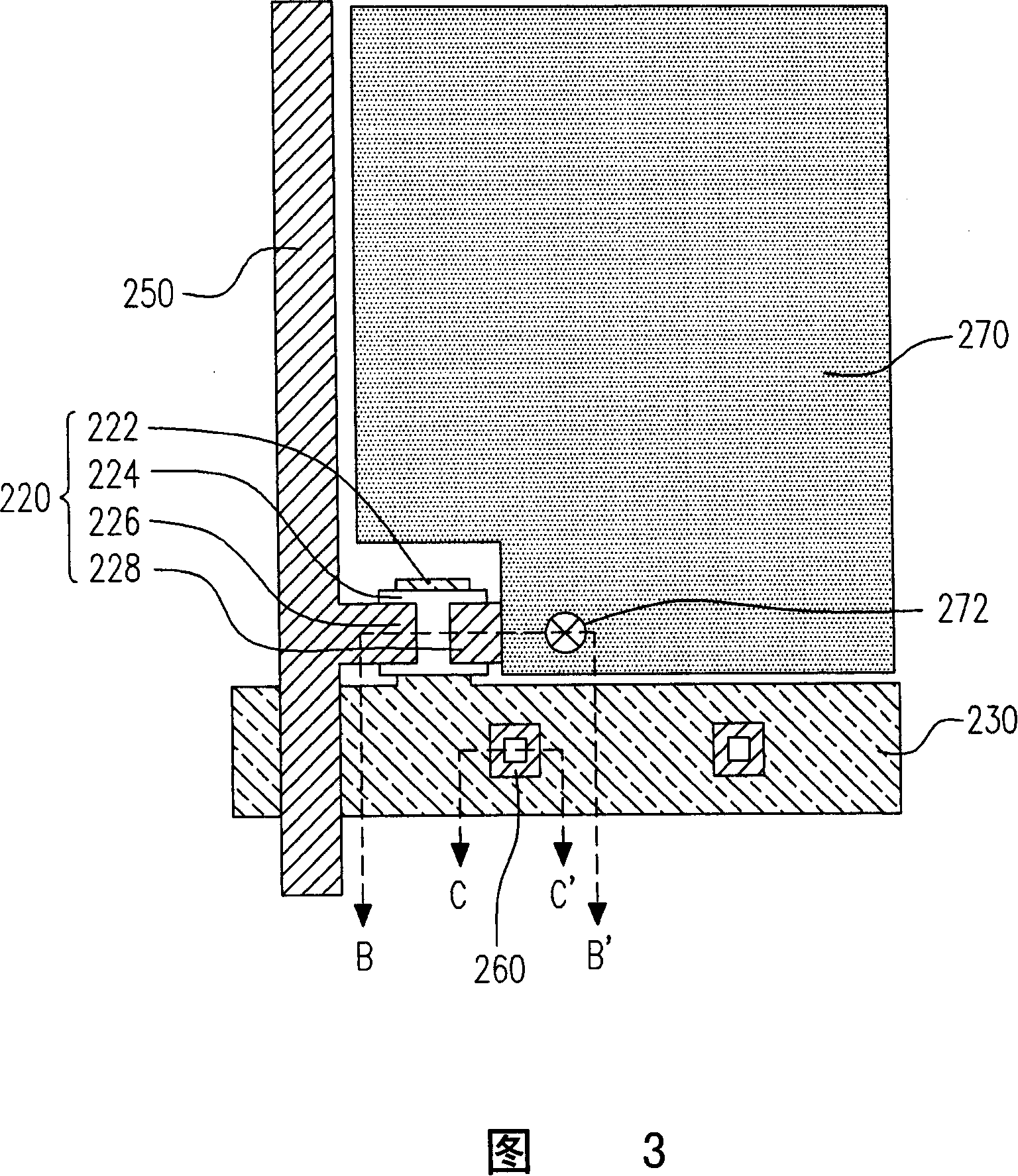
[0058] FIG. 7 is a cross-sectional view of a liquid crystal display panel according to yet another embodiment of the present invention. Please refer to FIG. 7 , this embodiment is similar to the above-mentioned first embodiment, the difference is that the retaining wall pattern 264 formed therein can be a structure composed of a lower layer 266 and an upper layer 268 . The steps of making this liquid crystal display panel 200" are to form the lower layer 266 of the wall pattern 264 at the same time when the channel layer 224 is formed on the insulating layer 240 above the grid 222 after the insulating layer 240 is formed. Therefore, the material of the lower layer 266 can be The same material as the channel layer 224. Then, when the source electrode 226 and the drain electrode 228 are formed on the channel layer 224, the upper layer 268 of the wall pattern 264 is formed simultaneously. Therefore, the material of the upper layer 268 can be the same as that of the source electrod...
no. 3 example
[0061] FIG. 8 is a schematic cross-sectional view of a liquid crystal display panel according to a third embodiment of the present invention. Please refer to FIG. 8, the liquid crystal display panel 800 includes a first substrate 810, a pixel array 820 and a color filter array 830 formed on the first substrate 810, wherein each pixel of the pixel array 820 includes a scanning line, a data line, a thin film transistor and a pixel electrode (not shown), the pixel structure can be any existing pixel structure. The color filter array 830 is disposed above the pixel array 820 , and the column spacer 860 is disposed above the color filter array 830 . In addition, the second substrate 815 is disposed opposite to the first substrate 810 , and the liquid crystal layer 870 is disposed between the first substrate 810 and the second substrate 815 . In particular, a plurality of protruding structures 840 are formed on the second substrate 815 to enable the liquid crystal display panel 800...
PUM
| Property | Measurement | Unit |
|---|---|---|
| Diameter | aaaaa | aaaaa |
Abstract
Description
Claims
Application Information
 - Generate Ideas
- Intellectual Property
- Life Sciences
- Materials
- Tech Scout
- Unparalleled Data Quality
- Higher Quality Content
- 60% Fewer Hallucinations
Browse by: Latest US Patents, China's latest patents, Technical Efficacy Thesaurus, Application Domain, Technology Topic, Popular Technical Reports.
© 2025 PatSnap. All rights reserved.Legal|Privacy policy|Modern Slavery Act Transparency Statement|Sitemap|About US| Contact US: help@patsnap.com