Encapsulation structure and its method for computer electric microphone
A technology of micro-electromechanical microphone and packaging structure, which is applied in the direction of micro-structure technology, micro-structure devices, and processing micro-structure devices, etc., which can solve the problems of increasing uncertainty and the inability to reduce the volume of the micro-chip microphone structure, so as to reduce the number of process steps , The effect of increasing the strength of the package structure
- Summary
- Abstract
- Description
- Claims
- Application Information
AI Technical Summary
Problems solved by technology
Method used
Image

Examples
no. 1 Embodiment
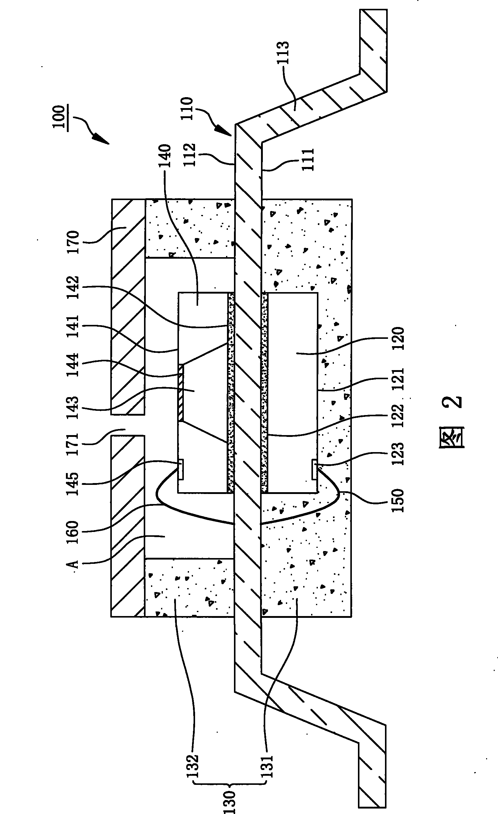
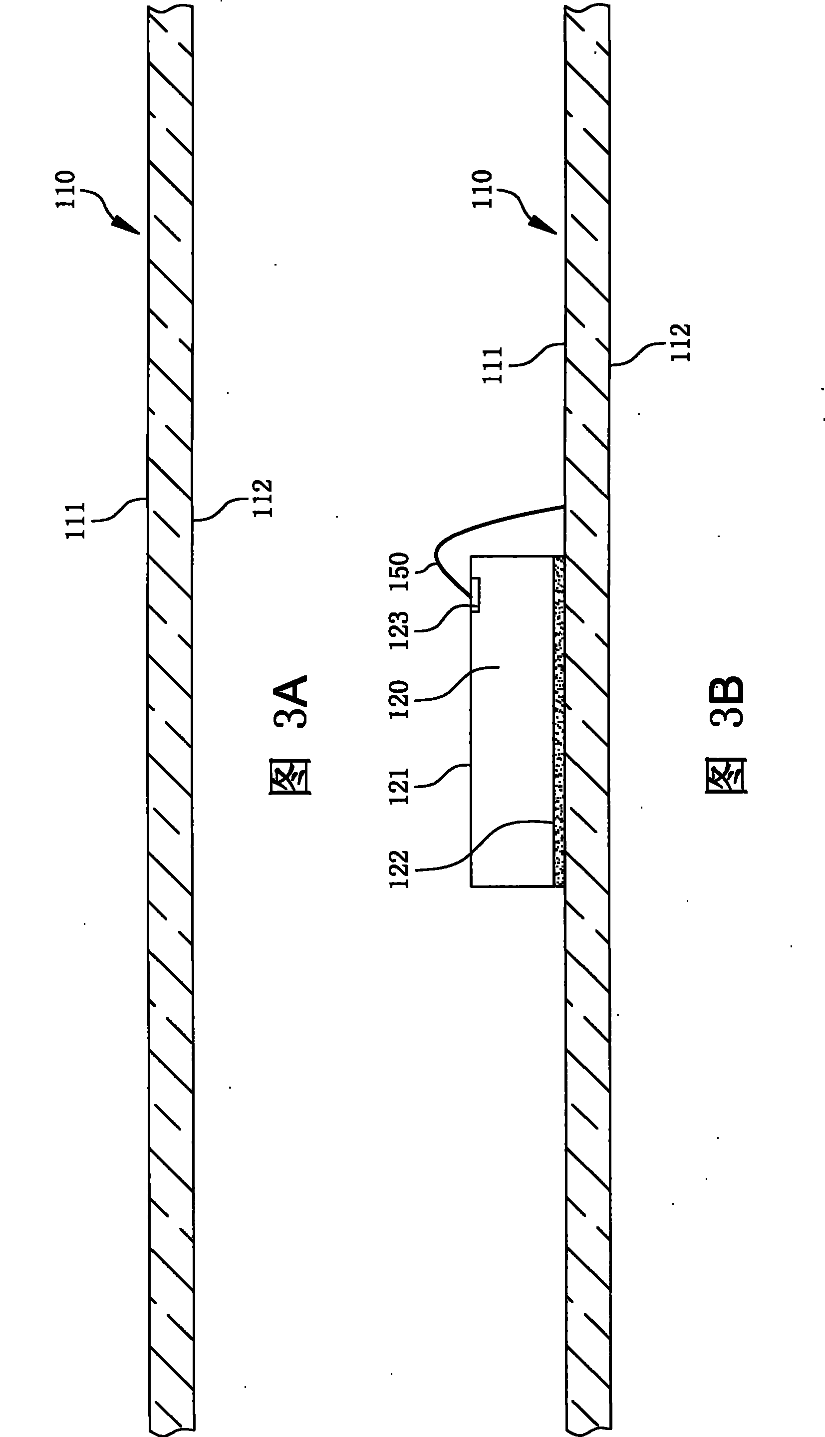
[0016] Please refer to FIG. 2 , according to the first embodiment of the present invention, a MEMS microphone package structure 100 is disclosed. The MEMS microphone package structure 100 includes a carrier 110, an application-specific chip 120, an encapsulant 130 and a microphone. Chip 140, the carrier 110 has a first surface 111 and a second surface 112, wherein the carrier 110 can be a packaging substrate or a lead frame, in this embodiment, the carrier 110 is a lead frame, the specific application The chip 120 is disposed on the first surface 111 of the carrier 110 and is electrically connected to the carrier 110. The application-specific chip 120 has an active surface 121, a back surface 122 and at least one pad 123. The application-specific chip 120 The back surface 122 is glued on the first surface 111 of the carrier 110, the pad 123 of the application-specific chip 120 is formed on the active surface 121 of the application-specific chip 120, and the MEMS microphone pack...
no. 2 Embodiment
[0018]In addition, please refer to FIG. 4 again, which is a second specific embodiment of the present invention, another MEMS microphone package structure 200, which includes a carrier 210, an application-specific chip 220, a package The colloid 230 and a microphone chip 240 . In this embodiment, the carrier 210 is a packaging substrate, the carrier 210 has a first surface 211 and a second surface 212, the first surface 211 is formed with a plurality of first connection pads 213 and a plurality of second The connection pad 214, the second surface 212 is formed with at least one third connection pad 215, the application-specific chip 220 is disposed on the first surface 211 of the carrier 210, and electrically connected to the carrier 210, the application-specific chip 220 has an active surface 221, a back surface 222 and several welding pads 223, the active surface 221 of the specific application chip 220 faces the first surface 211 of the carrier 210, and the MEMS microphone ...
PUM
 Abstract
Description
Claims
Application Information