Chip mounting and packaging structure and method
A packaging method and packaging structure technology, which is applied to semiconductor/solid-state device parts, semiconductor devices, electrical components, etc., can solve the problem that the adhesive fixed layer is difficult to take into account stress buffering and structural strength, etc., so that it is not easy to move and increase packaging Structural strength and uniform thickness
- Summary
- Abstract
- Description
- Claims
- Application Information
AI Technical Summary
Problems solved by technology
Method used
Image

Examples
Embodiment 1
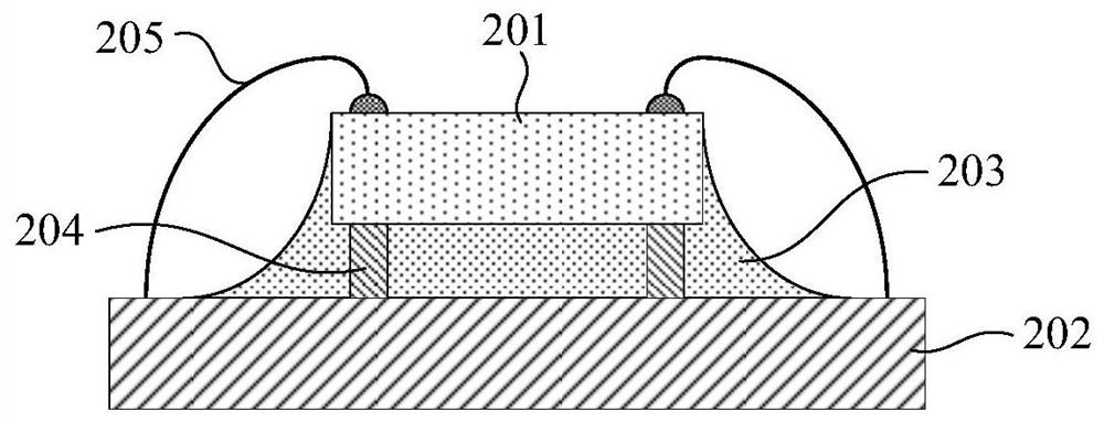
[0095] Embodiment 1: Die-attach packaging structure with height control layer
[0096] see Figure 3 to Figure 6 , an embodiment of the present invention provides a die-attach package structure, which is characterized in that it includes:
[0097] Substrate 202;
[0098] chip 201, the lower surface of which is pasted on the upper surface of the substrate 202 by adhesive;
[0099] Adhesive glue fixed layer 203, which is formed by curing the adhesive glue;
[0100] a height control layer structure 204, which is formed on the upper surface of the substrate 202 or the lower surface of the chip 201;
[0101] The bonding wire 205 is electrically connected to the chip 201 and the substrate 202 .
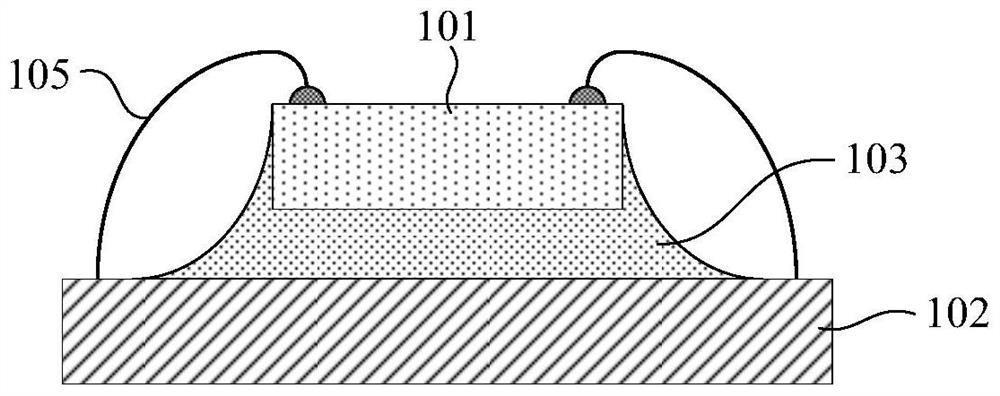
[0102] Such as image 3 As shown, it is a die-attach package structure provided by this embodiment. Wherein, the chip 201 may be a stress-sensitive chip such as a pressure sensor with a cavity structure, which is pasted on the upper surface of the substrate 202 by an adhesive. In thi...
Embodiment 2
[0109] Embodiment 2: Chip placement packaging method in which the height control layer structure is formed on the upper surface of the substrate
[0110] Such as Figure 7 to Figure 12 As shown, the present embodiment provides a chip placement and packaging method, which is characterized in that it includes the following steps:
[0111] 1) providing a substrate 302 and a chip 301;
[0112] 2) forming a height control layer structure 304 on the upper surface of the substrate 302;
[0113] 3) coating an adhesive 303a on the substrate 302;
[0114] 4) Paste the lower surface of the chip 301 on the upper surface of the substrate 302 through the adhesive;
[0115] 5) curing the adhesive glue 303a to form the adhesive glue fixed layer 303;
[0116] 6) Form bonding wires 305 on the upper surface of the chip 301 .
[0117] In step 1), see Figure 7 In step S1, a substrate 302 and a chip 301 are provided.
[0118] In step 2), see Figure 7 The S2 step and Figure 8 , forming a...
Embodiment 3
[0124] Embodiment 3: Chip placement packaging method in which the height control layer structure is formed on the lower surface of the chip
[0125] Such as Figure 13 to Figure 18 As shown, the present embodiment provides a chip placement and packaging method, which is characterized in that it includes the following steps:
[0126] 1) providing a substrate 402 and a chip 401;
[0127] 2) forming a height control layer structure 404 on the lower surface of the chip 401;
[0128] 3) coating the adhesive 403a on the substrate 402;
[0129] 4) Paste the lower surface of the chip 401 on the upper surface of the substrate 402 through the adhesive;
[0130] 5) curing the adhesive 403a to form an adhesive fixed layer 403;
[0131] 6) Form bonding wires 405 on the upper surface of the chip 401 .
[0132] In step 1), see Figure 13 In step S1, a substrate 402 and a chip 401 are provided.
[0133] In step 2), see Figure 13 The S2 step and Figure 14 , forming a height control ...
PUM
 Abstract
Description
Claims
Application Information