Layout structure of electrostatic discharge protecting circuit and its manufacturing method

A technology of electrostatic discharge protection and layout structure, which is applied in the direction of circuits, semiconductor/solid-state device manufacturing, electrical components, etc., can solve problems such as space utilization, and achieve the effects of improving efficiency, saving area, and reducing area

Inactive Publication Date: 2008-04-02
NOVATEK MICROELECTRONICS CORP
View PDF0 Cites 3 Cited by
  • Summary
  • Abstract
  • Description
  • Claims
  • Application Information

AI Technical Summary

Problems solved by technology

While these existing solutions solve the problem, they all require the use of additional space

Method used


Image

  • Layout structure of electrostatic discharge protecting circuit and its manufacturing method
  • Layout structure of electrostatic discharge protecting circuit and its manufacturing method
  • Layout structure of electrostatic discharge protecting circuit and its manufacturing method

Examples


Embodiment Construction

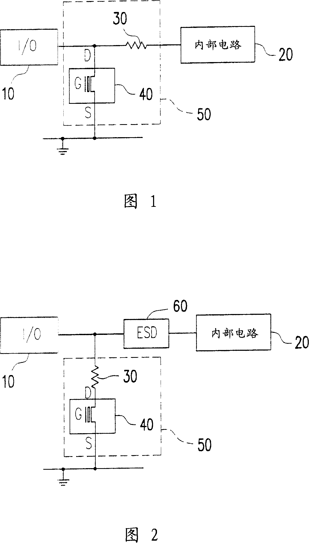
[0045] 1 and 2 are circuit diagrams of an electrostatic discharge protection circuit. Here, a field oxide device (FOD transistor for short) 40 is used as a protection component of the ESD protection circuit 50 . As shown in FIG. 1, in the electrostatic discharge protection circuit 50, a resistor 30 is coupled between the input / output pad (I / O pad) 10 and the internal circuit 20, wherein the resistor 30 is a current limiting resistor, which is used for The electrostatic discharge current is prevented from flowing into the internal circuit 20 through the bonding pad 10 . The drain D of the FOD transistor 40 is coupled between the bonding pad 10 and the resistor 30 , the source S of the FOD transistor 40 is grounded, and the gate G is in a floating state. Therefore, when electrostatic discharge occurs, the electrostatic discharge protection circuit 50 provides an electrostatic discharge current path from the bonding pad 10 to the ground, thereby preventing the internal circuit 2...


PUM


Abstract

The invention discloses an arrangement of an ESD protection circuit and a method for manufacturing the same. The ESD protection circuit comprises a substrate, a protection component and a resistor, wherein, the resistor is arranged in the region of the protection component, in part or whole area. As a result, the occupied area by the resistor is reduce and the junction parasitic capacitor generated inside the protection component, thereby reducing the manufacture cost of the ESD protection circuit and the influence of the ESD protection circuit on the whole internal circuit to the lowest.

Description

technical field [0001] The invention relates to an electrostatic discharge protection circuit and a manufacturing method thereof, in particular to a layout structure for an electrostatic discharge protection circuit on an integrated circuit and a manufacturing method thereof. Background technique [0002] The main structure of the electrostatic discharge protection circuit includes a protective component and a resistor, wherein the resistor is a current-limiting resistor, and this structure can effectively improve the ability of electrostatic discharge (ESD) protection. The layout design of the existing electrostatic discharge protection circuit is shown in FIG. 11 , in which the resistor 30 is arranged outside the protection component 40 , so the resistor 30 needs to occupy an additional area. In addition, this layout results in a large overlapping area between the drain D and the substrate in the protection element 40 , thereby forming a large parasitic capacitance. Exces...

Claims


Application Information

Patent Timeline
Patent Type & Authority Applications(China)
IPC IPC(8): H01L27/02H01L23/60H01L21/82
Inventor 江雪莉李彦枏
Owner NOVATEK MICROELECTRONICS CORP
Why Eureka
Try Eureka