Semiconductor laser device, its manufacturing method and optical pickup head device using the same

A laser device and semiconductor technology, applied in the direction of semiconductor lasers, semiconductor devices, optical recording heads, etc., can solve problems such as difficult heat dissipation of light-emitting elements, damage to the reliability of semiconductor laser devices, and deterioration of light-emitting elements, etc., to achieve miniaturization , prolong life, and prevent deterioration

Inactive Publication Date: 2008-04-02
SHARP KK
View PDF2 Cites 4 Cited by
  • Summary
  • Abstract
  • Description
  • Claims
  • Application Information

AI Technical Summary

Problems solved by technology

However, it is difficult to dissipate the heat generated by the light-emitting element sufficiently because it is only dissipated from the case body. Therefore, if the semiconductor laser device is used for a long time, the light-emitting element will gradually deteriorate, which may damage reliability and shorten the life.
In addition, since the optical axis of the emitted light from the light emitting element is deflected due to the influence of the deformation of the housing through the substrate lead and the frame, the reliability of the semiconductor laser device is impaired.
[0006] In addition, the semiconductor laser device 20 shown in FIG. 8 is fixed on a surface perpendicular to the optical axis of the outgoing light from the semiconductor laser device 20, so by adjusting the position of the through hole provided on the housing, it can be aligned with the outgoing light. The position adjustment is performed on the plane perpendicular to the optical axis of the emitted light, but the position adjustment in the direction of light emission, that is, the adjustment of the optical path length from the emitting position of the laser to the irradiation position cannot be performed.

Method used


Image

  • Semiconductor laser device, its manufacturing method and optical pickup head device using the same
  • Semiconductor laser device, its manufacturing method and optical pickup head device using the same
  • Semiconductor laser device, its manufacturing method and optical pickup head device using the same

Examples


Embodiment Construction

[0058] Preferred embodiments of the present invention will be described in detail below with reference to the drawings.

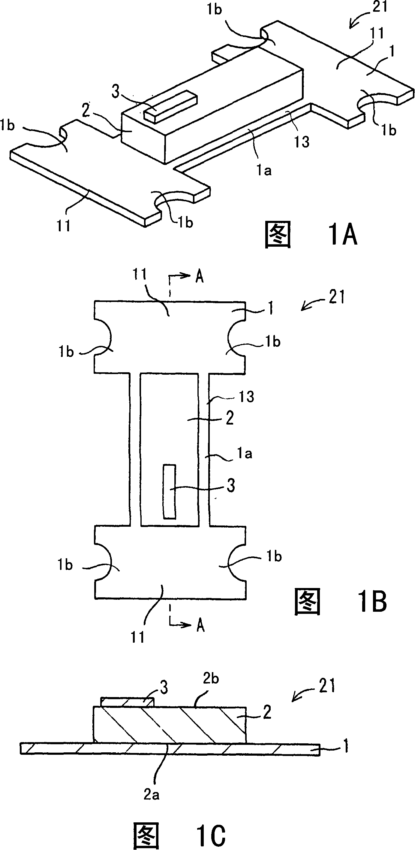
[0059] 1A is a perspective view showing a semiconductor laser device 21 according to a first embodiment of the present invention, FIG. 1B is a plan view, and FIG. 1C is a cross-sectional view taken along line A-A of FIG. 1B . The semiconductor laser device 21 includes a flat plate 1 , a bulk body 2 , and a laser chip 3 . The flat plate 1 is a member for joining with the housing, and includes: a rectangular joining portion 1a joined to the block 2; The exposed part 11. That is, the exposed portion 11 is provided on the flat plate 1 in which a part of one side surface joined to the block body 2 is exposed. The block 2 is formed in a rectangular parallelepiped, and is joined to a surface perpendicular to the thickness direction of the joining portion 1 a of the flat plate 1 . The laser chip 3 is bonded to the surface 2 b of the bulk body 2 opposite to the s...


PUM

PropertyMeasurementUnit
wavelengthaaaaaaaaaa

Abstract

There is provided a semiconductor laser apparatus capable of sufficiently discharging heat generated at a semiconductor laser element, having a simple manufacturing step, and capable of adjusting an optical path length, as well as a method for manufacturing the same. A laser chip is connected through a block and a plate to a housing. Further, the plate is partially exposed from a connecting surface between the block and the plate, and when disposed in the housing, the semiconductor chip and the block are inserted from an outside of the housing to an inside thereof, and the plate is exposed outwardly from the housing. An optical axis of an output light beam from the laser chip is in parallel to a ground plane of the housing.

Description

technical field [0001] The present invention relates to a semiconductor laser device suitable for being installed in an optical disc recording and reproducing device, its manufacturing method and an optical pick-up head device using the device. Background technique [0002] In an optical drive such as a CD (Compact Disc) drive or a DVD (Digital Versatile Disc) drive, an optical pickup device for recording and reproducing data includes a semiconductor laser element as a light source and a light receiving element that receives reflected light from the disc. And constitute. The laser light emitted from the light source is adjusted so that the light spot on the CD or DVD recording surface is minimized. The laser light reflected on the recording surface is received by a photodetector and converted into data. [0003] Lasers with a wavelength of 790nm are used for CDs, lasers with a wavelength of 650nm are used for DVDs, and lasers with a wavelength of 405nm are used for next-ge...

Claims


Application Information

Patent Timeline
Patent Type & Authority Applications(China)
IPC IPC(8): H01S5/00G11B7/125H01S5/0232
CPCH01S5/02244H01S5/02248H01L2224/48137G11B7/127H01L24/97H01L2224/48091H01S5/02325H01S5/0232H01L2924/00014
Inventor 福本悟金子延容
Owner SHARP KK
Why Eureka
Try Eureka