

Semiconductor integrated circuit device and receiving device
A technology of integrated circuits and receiving devices, which is applied in the structural field of high-frequency front-end parts, can solve problems such as changes in the direction of reflected waves, and achieve the effects of reducing the number of components, improving performance, reducing manufacturing costs or installation area
- Summary
- Abstract
- Description
- Claims
- Application Information
AI Technical Summary
Problems solved by technology
Method used
Image

Examples
Embodiment approach 1
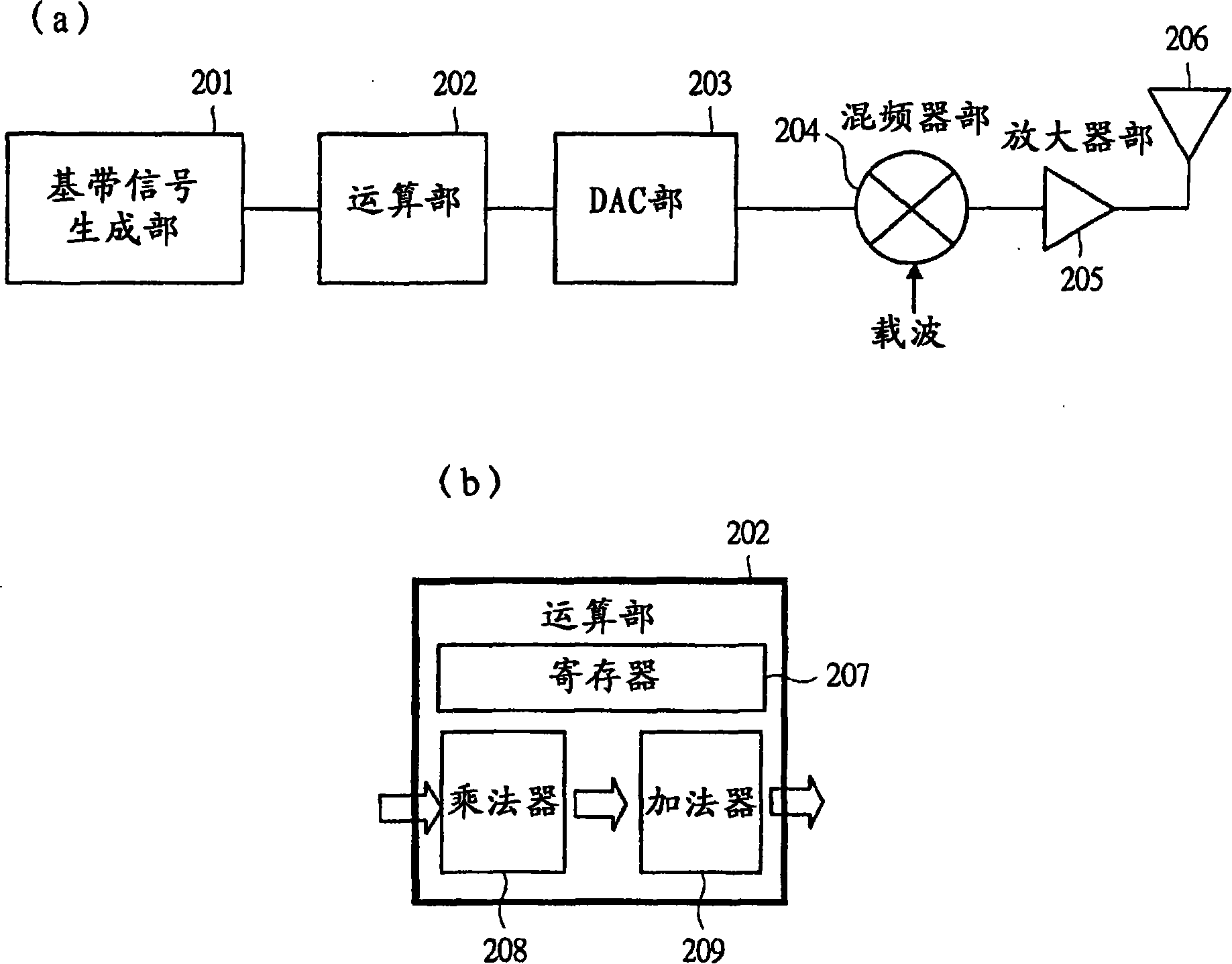
[0103] figure 2 (a) is a block diagram showing the configuration of the semiconductor integrated circuit device according to Embodiment 1 of the present invention, figure 2 (b) means figure 2 (a) is a block diagram showing the configuration of the calculation unit 202 .
[0104] First, through figure 2 An example of the configuration of the semiconductor integrated circuit device according to the first embodiment will be described. The semiconductor integrated circuit device according to Embodiment 1 is used, for example, as a semiconductor integrated circuit device (IC) used in a wireless transmitter such as a reader / writer in a UHF frequency band electronic tag (RFID) system. formed on a semiconductor chip. This semiconductor integrated circuit device having a wireless transmitter function is composed of, for example, a baseband signal generating unit 201 that generates data for transmission; and a multiplier 208, an adder 209, and a register 207 to control the degre...
Embodiment approach 2
[0120] Figure 4 It is a block diagram showing the structure of the semiconductor integrated circuit device according to Embodiment 2 of the present invention.
[0121] The semiconductor integrated circuit device of the second embodiment is an example in which the digital filter 401 is inserted between the baseband signal generation unit 201 and the DAC unit 203 compared to the semiconductor integrated circuit device of the first embodiment described above.
[0122] Both the calculation unit 202 and the digital filter 401 are logic operations, and it does not matter which one is executed first. Thus, either Figure 4 (a) After adding the digital filter 401 after the calculation unit 202, it can also be as Figure 4 As in (b), a digital filter 401 is added before the arithmetic unit 202 .
[0123] By adding a digital filter, the rising and falling waveforms become smoother.
Embodiment approach 3
[0125] Figure 5 It is a block diagram showing the structure of the semiconductor integrated circuit device according to Embodiment 3 of the present invention.
[0126] The semiconductor integrated circuit device of Embodiment 3 is compared to the semiconductor integrated circuit device of Embodiment 2 above ( Figure 4 (a)) is an example in which a circulator 501 for separating a transmission signal and a reception signal, a reception section 502 for receiving a modulated wave, a demodulation section 503 for extracting raw data from a modulated wave, and a reception state judgment section 504 for judging a reception state are added .
[0127] Based on the raw data demodulated by the demodulation unit 503, a determination is made in the reception state determination unit 504, and the calculation coefficient in the register 207 is changed based on the determination result.
[0128] In a communication system that implements backscatter communication, the transmission state (mo...
PUM
 Abstract
Description
Claims
Application Information