Flat fluorescent lamp

A fluorescent lamp, flat technology, applied to the parts of gas discharge lamps, etc., can solve the problems of poor productivity, high circuit design cost, and difficult to control the thickness of the dielectric layer.

Inactive Publication Date: 2008-04-30
DELTA OPTOELECTRONICS +1
View PDF0 Cites 0 Cited by
  • Summary
  • Abstract
  • Description
  • Claims
  • Application Information

AI Technical Summary

Problems solved by technology

However, in the manufacturing process of this flat fluorescent lamp, the method of forming the dielectric layer by multi-layer screen printing is relatively complicated, and the yield is not good.
Furthermore, the thickness of the dielectric layer formed by multi-layer screen printing is not easy to control, resulting in insufficient and uneven brightness between different flat fluorescent lamps or in different areas of a single flat fluorescent lamp
Therefore, the cost of the circuit design of the traditional flat fluorescent lamp is relatively high

Method used


Image

  • Flat fluorescent lamp
  • Flat fluorescent lamp
  • Flat fluorescent lamp

Examples


no. 1 example

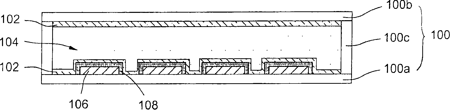
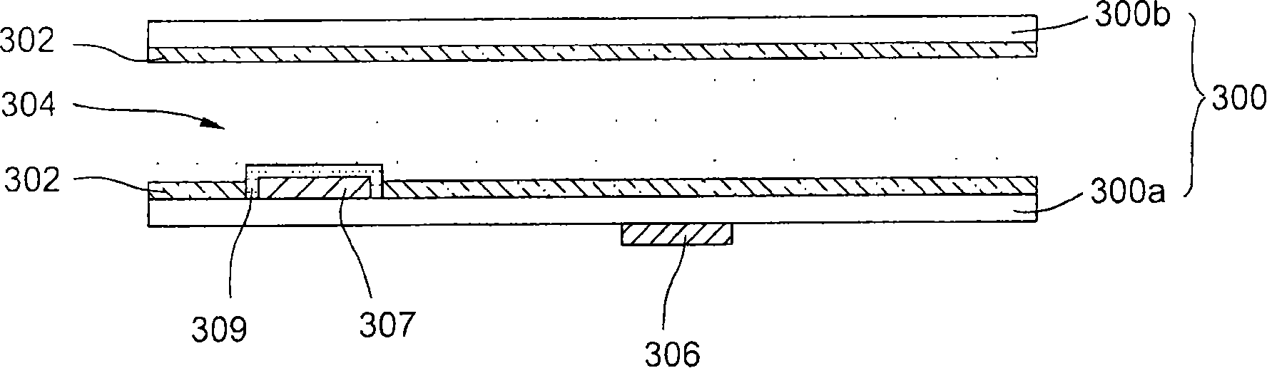
[0037] figure 2 A cross-sectional view showing a flat fluorescent lamp according to a first preferred embodiment of the present invention. Please refer to figure 2 The flat fluorescent lamp of this embodiment is mainly composed of a lower substrate 300a, an upper substrate 300b, a phosphor 302, a discharge gas 304, and a plurality of first electrodes 306 and second electrodes 307. Among them, a gas discharge chamber 300 is formed between the lower substrate 300a and the upper substrate 300b and is filled with a discharge gas 304; the first electrode 306 is located on the outer surface of the lower substrate 300a; the second electrode 307 is located on the inner surface of the lower substrate 300a and has a dielectric The layer 309 covers the second electrode 307 ; and the phosphor 302 is disposed on the inner wall of the gas discharge chamber 300 .

[0038] In this embodiment, since the paired electrodes 306 and 307 are located on different planes, the discharge area is la...

no. 2 example

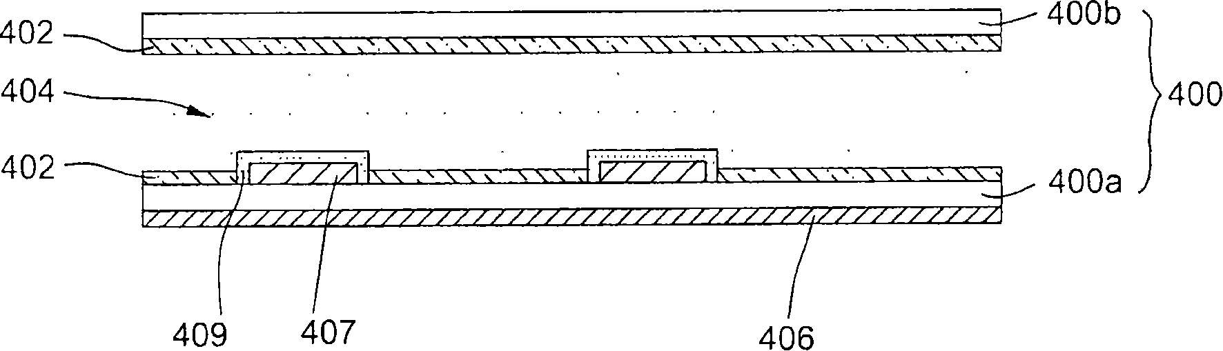
[0042] Figure 3AA cross-sectional view showing a flat fluorescent lamp according to a second preferred embodiment of the present invention. Please refer to Figure 3A , The flat fluorescent lamp of this embodiment is composed of a lower substrate 400a, an upper substrate 400b, a phosphor 402, a discharge gas 404, a first electrode 406 and a second electrode 407. In this embodiment, a gas discharge cavity 400 is formed between the lower substrate 400a and the upper substrate 400b and filled with discharge gas 404; the first electrode 406 is located on the outer surface of the lower substrate 400a; the second electrode 407 is located on the inner surface of the lower substrate 400a and covered with a dielectric layer 409 ; and the phosphor 402 is disposed on the inner wall of the gas discharge chamber 400 .

[0043] Figure 3B and Figure 3C A schematic diagram showing the change of the first electrode in the flat fluorescent lamp according to the second preferred embodimen...

no. 3 example

[0045] Figure 4 A cross-sectional view showing a flat fluorescent lamp according to a third preferred embodiment of the present invention. Figure 4 The flat fluorescent lamp shown includes a lower substrate 500 a , an upper substrate 500 b , a phosphor 502 , a discharge gas 504 , a first electrode 506 and a second electrode 507 . In this embodiment, a gas discharge cavity 500 is formed between the lower substrate 500a and the upper substrate 500b and is filled with a discharge gas 504; the first electrode 506 is located on the outer surface of the lower substrate 500a; and the second electrode 507 is formed inside the lower substrate 500a. The surface is covered with a dielectric layer 509; and the phosphor 502 is disposed on the inner wall of the gas discharge chamber 500;

[0046] In this embodiment, a carrier substrate 510 is disposed below the lower substrate 500a, and the carrier substrate 510 can optionally be attached to the lower substrate 500a with an adhesive 508 ...


PUM


Abstract

A flat fluorescent lamp is disclosed. The flat fluorescent lamp comprises a gas discharge chamber, a fluorescent substance, a discharge gas, and a plurality of first and second electrodes. The fluorescent substance is disposed on an inner surface of the gas discharge chamber and the discharge gas is filled in the gas discharge chamber. An electrode pair includes the first and the second electrodes. The first and the second electrodes are disposed on different planes so that the discharge area formed between the first and the second electrodes is larger than that formed between the two electrodes on a same plane to perform better efficiency of luminance.

Description

technical field [0001] The invention discloses a flat fluorescent lamp structure, in particular to a flat fluorescent lamp structure in which electrodes are located inside and outside a gas discharge chamber. Background technique [0002] In recent years, liquid crystal display panels (LCD panels) have gradually become the mainstream of display screens of general televisions. Since the liquid crystal display panel itself does not have the function of emitting light, a backlight module (backlight module) must be arranged under the liquid crystal display panel to provide light source to achieve the display function. The light sources of the backlight modules of commercially available TVs are composed of a large number of cold cathode tubes (CCFLs), and some light emitting diodes (LEDs) are also used as light sources. However, since CCFLs or LEDs are linear or point light sources, the diffusion plate in the backlight module is required to achieve uniform lighting effect. [0...

Claims


Application Information

Patent Timeline
Patent Type & Authority Applications(China)
IPC IPC(8): H01J61/02H01J61/04H01J61/35H01J61/38H01J61/16
Inventor 谢宇恒李建兴陈照勗陈来成
Owner DELTA OPTOELECTRONICS
Why Eureka
Try Eureka