Semiconductor device
A semiconductor, conductive type technology, applied in the direction of semiconductor devices, semiconductor/solid-state device components, electric solid-state devices, etc., can solve the problem of limited chip size miniaturization, prevent reliability degradation, ensure pad size, improve area effect
- Summary
- Abstract
- Description
- Claims
- Application Information
AI Technical Summary
Problems solved by technology
Method used
Image

Examples
Embodiment Construction
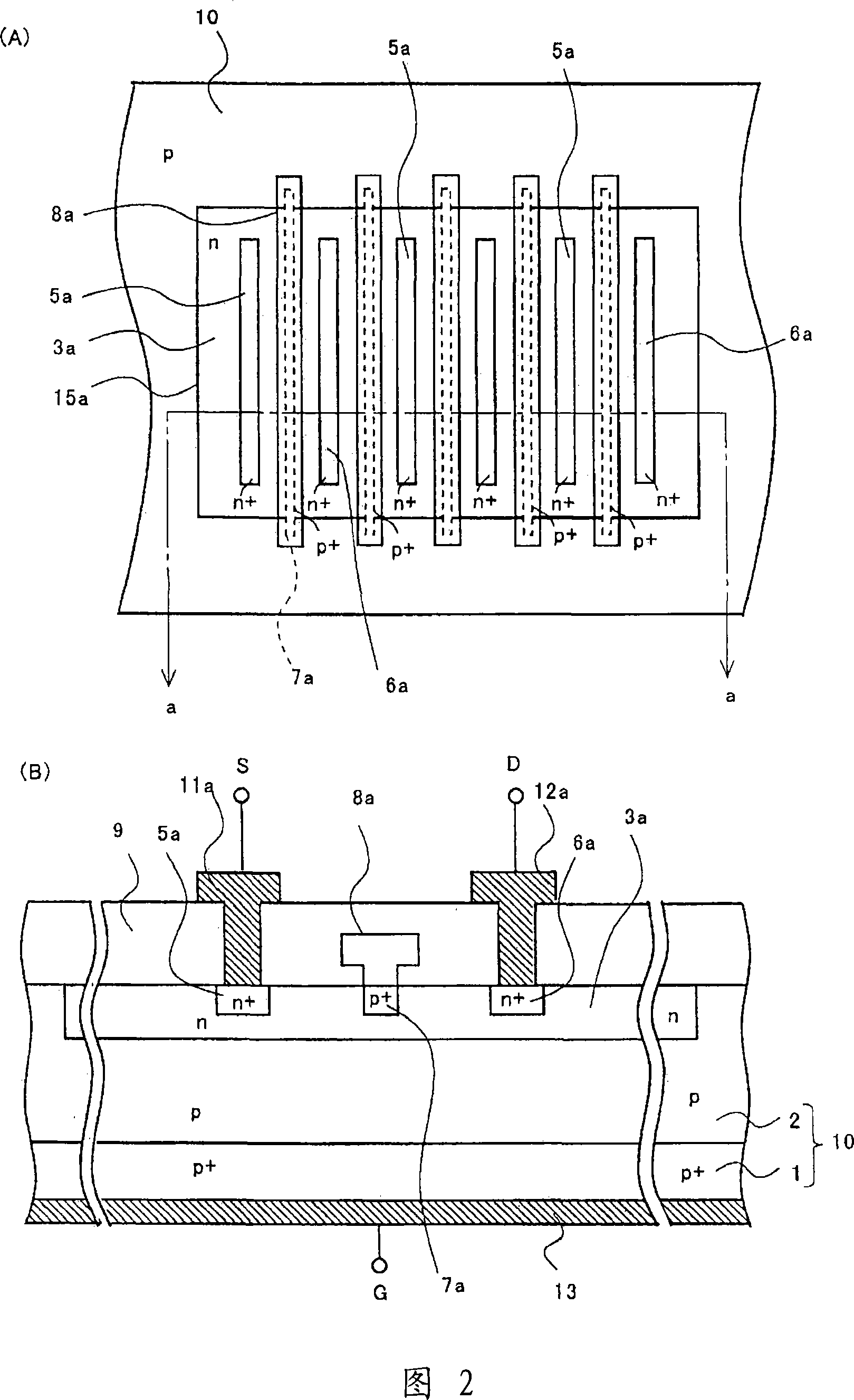
[0061] Next, an embodiment of the present invention will be described with reference to FIGS. 1 to 5 . In addition, the semiconductor device of this embodiment is applicable to a junction field effect transistor (Junction FET (Field Effect Transistor): hereinafter referred to as J-FET) that uses more than one pn junction depletion layer biased in the reverse direction to change the cross-sectional area of the channel. ), and the J-FET is taken as an example below.
[0062] First, a first embodiment of the present invention will be described with reference to FIGS. 1 and 2 .
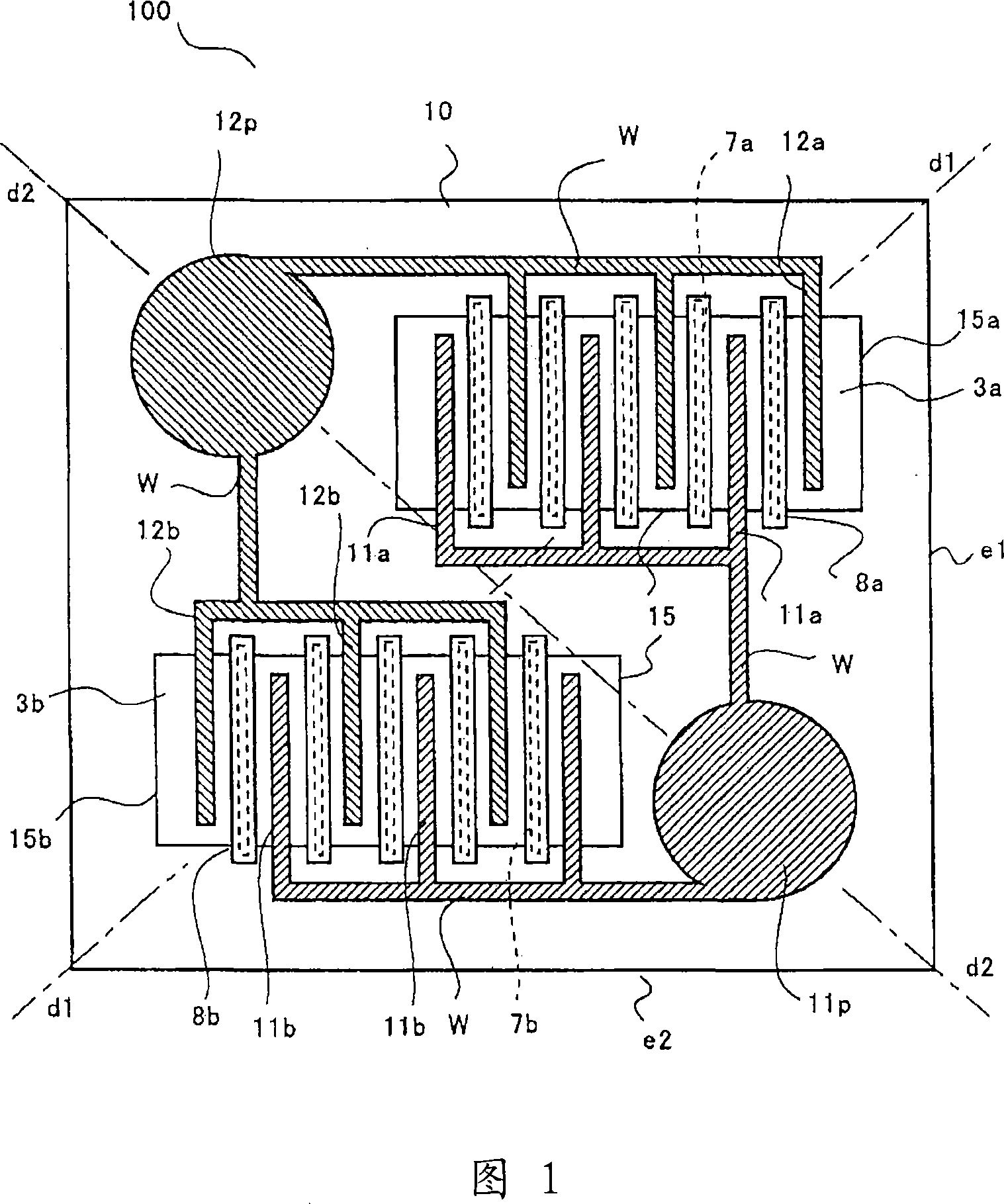
[0063] FIG. 1 is a plan view showing a J-FET of the first embodiment. The J-FET in this embodiment is composed of a conductive semiconductor substrate, a first action area, a second action area, a first pad electrode, and a second pad electrode.
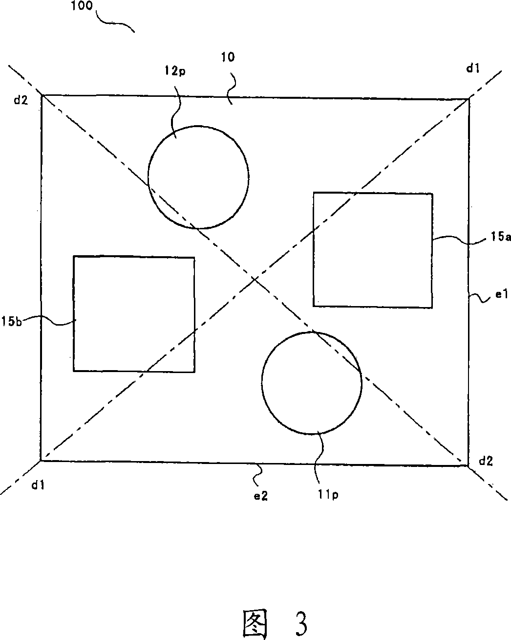
[0064] In J-FET 100, two operating regions 15 (first operating region 15a and second operating region 15b) are provided on semiconductor substrate 10 consti...
PUM
 Abstract
Description
Claims
Application Information
 - R&D Engineer
- R&D Manager
- IP Professional
- Industry Leading Data Capabilities
- Powerful AI technology
- Patent DNA Extraction
Browse by: Latest US Patents, China's latest patents, Technical Efficacy Thesaurus, Application Domain, Technology Topic.
© 2024 PatSnap. All rights reserved.Legal|Privacy policy|Modern Slavery Act Transparency Statement|Sitemap