Estimation method for integrate circuit function yield

A technology of integrated circuit and yield rate, which is applied in the field of integrated circuit function yield estimation, and can solve problems such as yield estimation error

Inactive Publication Date: 2008-05-14
XIDIAN UNIV
View PDF0 Cites 9 Cited by
  • Summary
  • Abstract
  • Description
  • Claims
  • Application Information

AI Technical Summary

Problems solved by technology

In terms of yield estimation method, the traditional circular defect mod

Method used


Image

  • Estimation method for integrate circuit function yield
  • Estimation method for integrate circuit function yield
  • Estimation method for integrate circuit function yield

Examples


Embodiment Construction

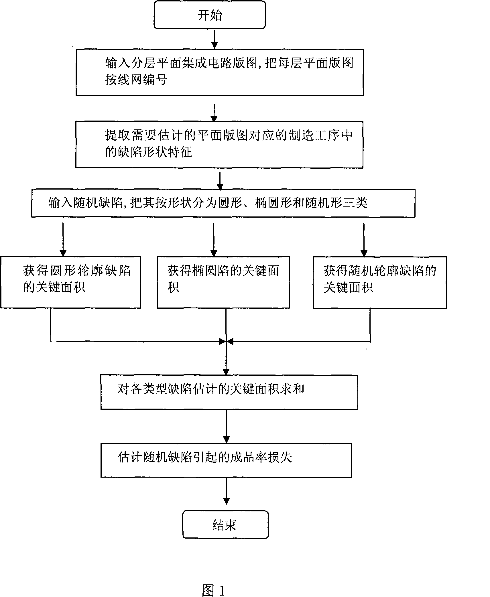
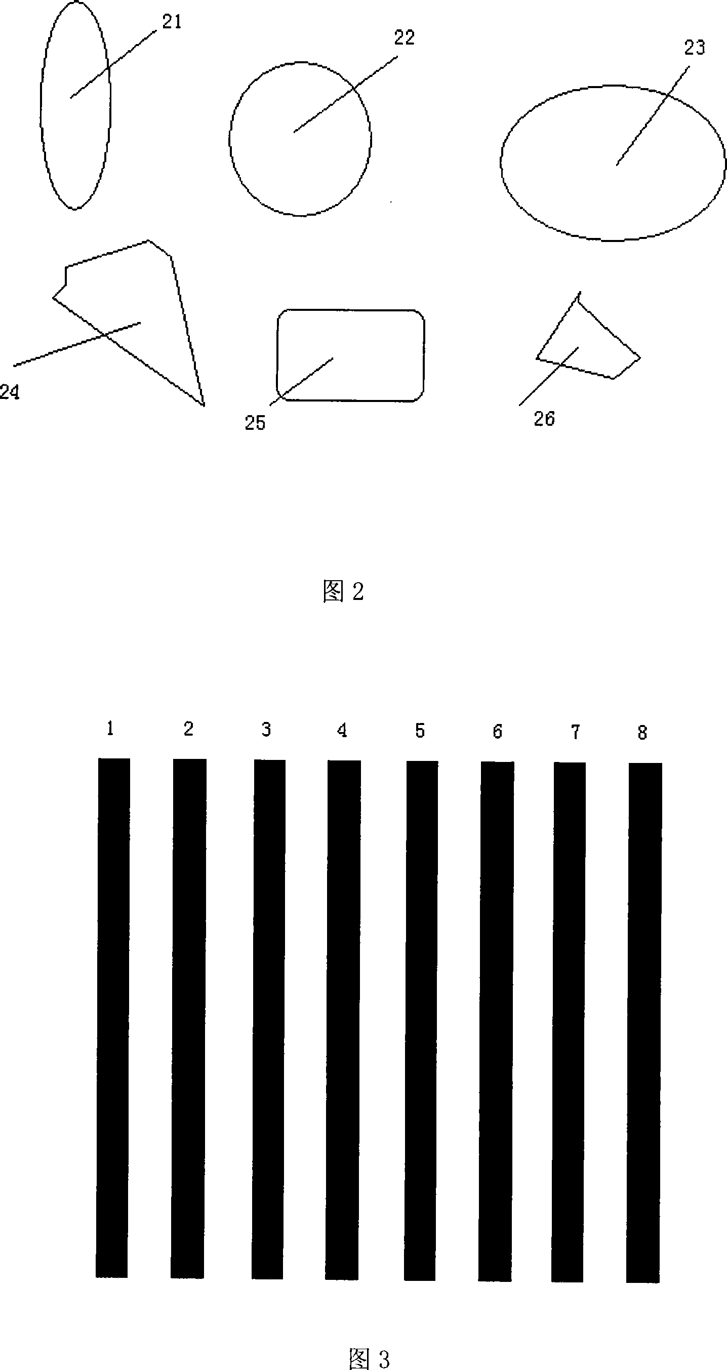
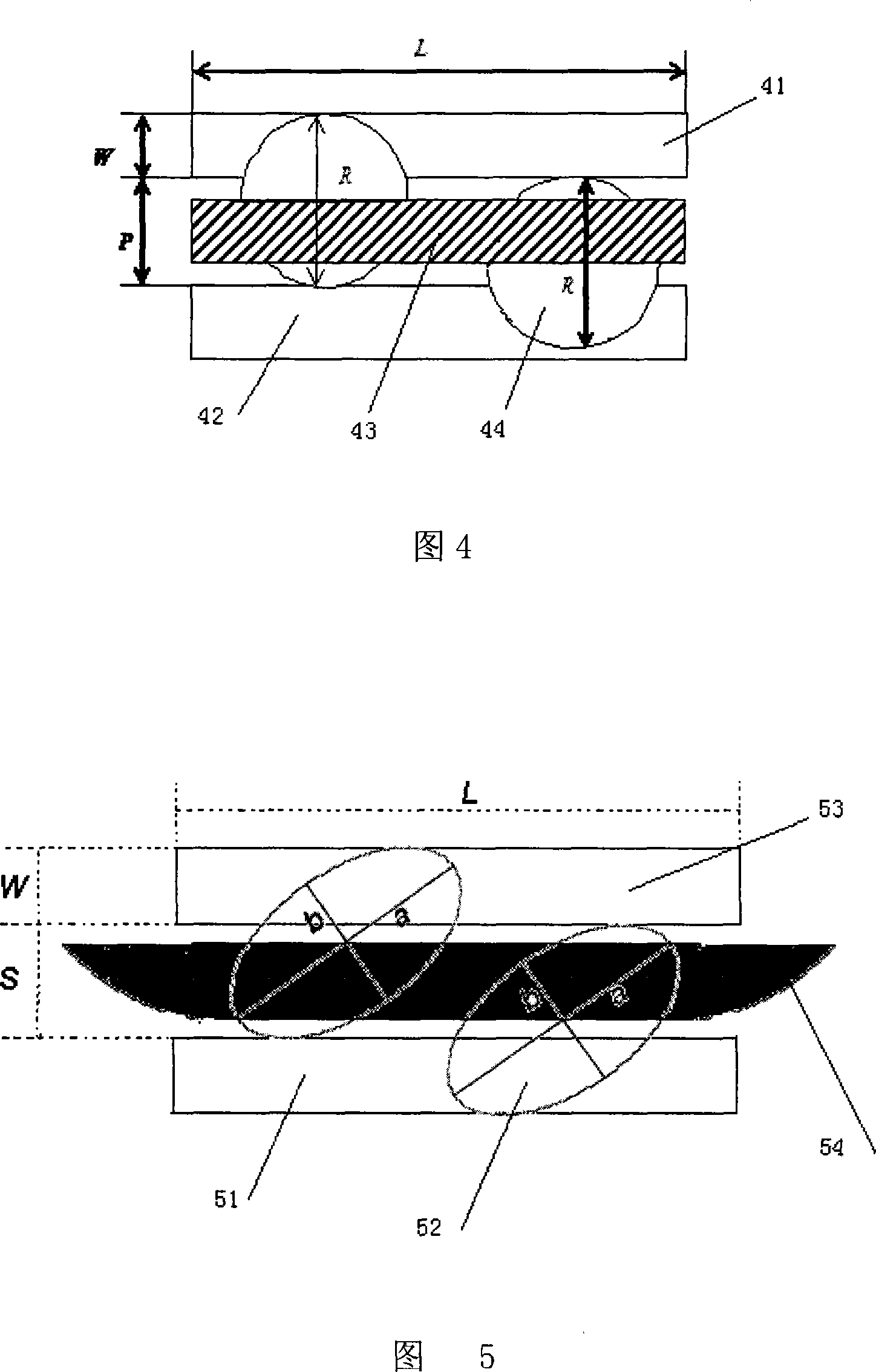
[0059] The yield estimation method implemented in the present invention is to analyze the defect parameters on the basis of collected defect characteristic parameters related to process function yield, and then estimate the functional yield of different process layers according to the layout of the input integrated circuit chip. The defect characteristic parameters of the functional yield related to the i-th layer process generally include defect shape, defect density D i , the defect spatial distribution characteristic is the defect clustering coefficient α i , these parameters are collected and stored in the engineering database. In the embodiment of the present invention, according to the type of the analyzed defect data, that is, a set of formulas can accurately estimate the functional yield of the integrated circuit, and the specific process is shown in FIG. 1 .

[0060] With reference to Fig. 1, the process of the integrated circuit function yield estimation method of t...


PUM


Abstract

The invention discloses a function pass rate estimating method for an integrated circuit, aiming at solving the problem of low accuracy of the existing estimating method. Adopting different pass rate estimating methods for different types of errors, the invention comprises the steps as follows: each layer of plane layout of the to-be-estimated integrated circuits is numbered according to wire mesh; the error shape feature is extracted in production procedures corresponding to of the plane layout of the to-be-estimated integrated circuits; the error shape feature is divided into three grades of a circular outline, an elliptic outline and a random outline; the key areas of the errors of the circular outline, the elliptic outline and the random outline are calculated on a selected plane layout respectively, summing up to gain the total key area of the three errors on the selected plane layout; the pass rate of corresponding processes and the pass rate of the integrated circuit in the selected plane layout are estimated by utilizing a normal method according to the total sum. The invention characterized by high estimating accuracy is applicable for affirmation about the pass rate loss estimation of chips caused by the errors of random shape during the producing process.

Description

technical field [0001] The present invention relates to the estimation of functional yields caused by random defects in IC (integrated circuit) manufacturing, and more precisely, to methods for determining chip yield losses caused by randomly shaped defects in the manufacturing process, the results of which can be used to predict and improve Yield of integrated circuit chips. Background technique [0002] Yield estimates are an important indicator of profitability for semiconductor fabs. For newly introduced process lines, the yield rate is generally only 20%. In order to ensure the benefit of the manufacturing plant, the reasons for the loss of yield should be quickly analyzed. In the investigation of the cause of yield loss, accurate estimation of yield is the premise. For a mature process line, before chip development and mass production, through accurate estimation of the yield, measures such as changing the layout shape, design rules and process conditions can maximi...

Claims


Application Information

Patent Timeline
IPC IPC(8): G06T7/00
Inventor 王俊平郝跃孙晓丽铁满霞任春丽张俊明张宇王瑞岩郭清衍周海
Owner XIDIAN UNIV
Why Eureka
Try Eureka