Mounting device, plasma processing apparatus and plasma processing method
A plasma and carrier technology, applied in the directions of plasma, chemical instruments and methods, cleaning methods and utensils, etc., to achieve the effects of increased durability and high plasma resistance
Inactive Publication Date: 2008-05-14
TOKYO ELECTRON LTD
View PDF2 Cites 9 Cited by
- Summary
- Abstract
- Description
- Claims
- Application Information
AI Technical Summary
Problems solved by technology
Regarding these problems, nothing is described in Patent Document 2
Method used
View moreImage
Smart ImageViewing Examples

Examples
Embodiment
[0066] Experiments performed to confirm the effects of the present invention will be described.
Login to View More PUM
| Property | Measurement | Unit |
|---|---|---|
| thickness | aaaaa | aaaaa |
| surface roughness | aaaaa | aaaaa |
| surface roughness | aaaaa | aaaaa |
Abstract
The invention provides a mounting device which has no heavy metallic pollution on the processed object, and is unable to cause insulation damage after a long-time static chuck. The invention is made by adopting the static chuck which is used as the insulation layer of the surface of the electrode layer through plasma spray plating, consisting of an yttria spray plating layer whose thickness is 200um to 280um. The surface of the invention is formed with a structure depending on the surface rough degree of the grain diameter of the spray plated yttria. The structure can increase the durability of the plasma without causing any heavy metallic pollution.
Description
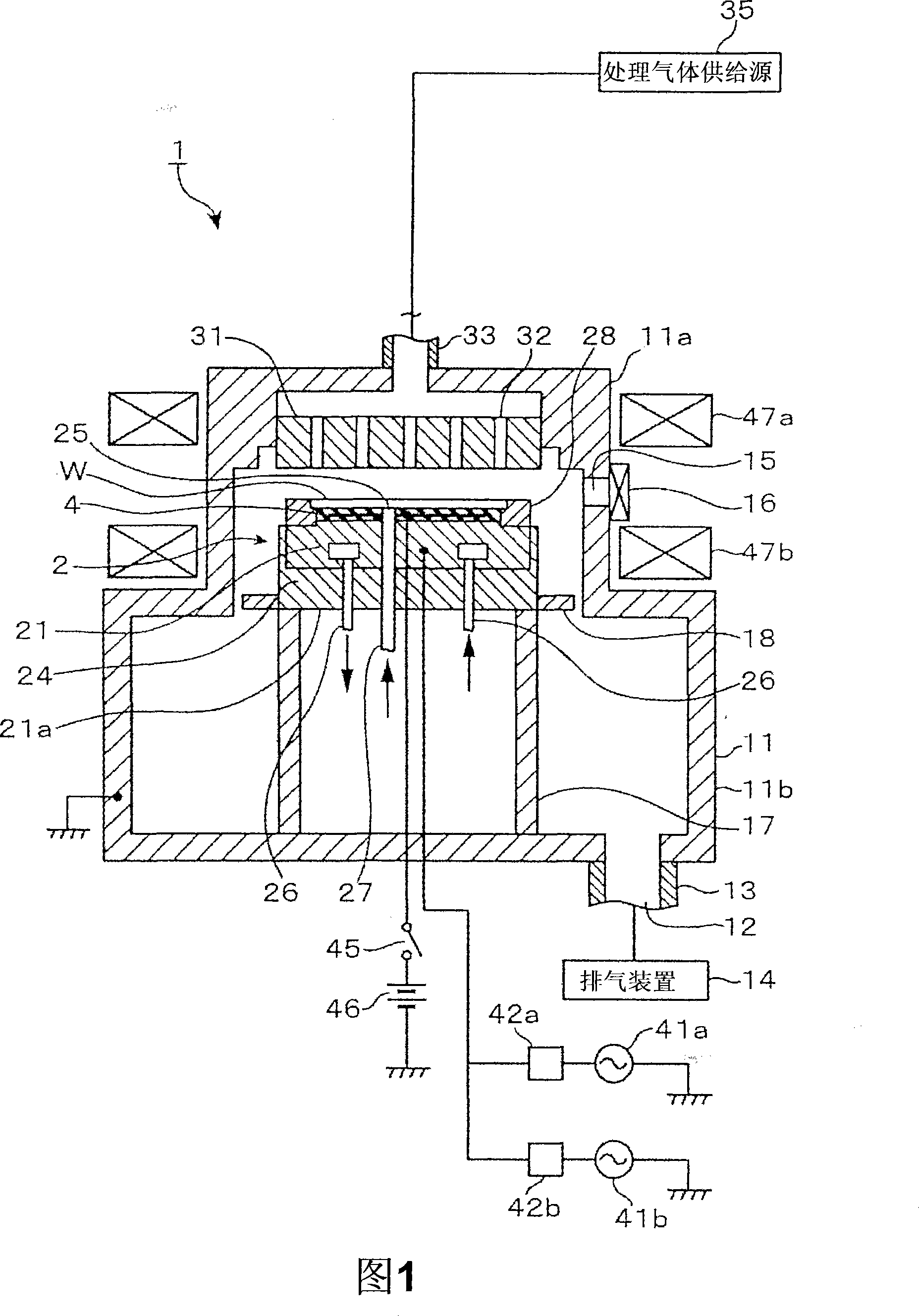
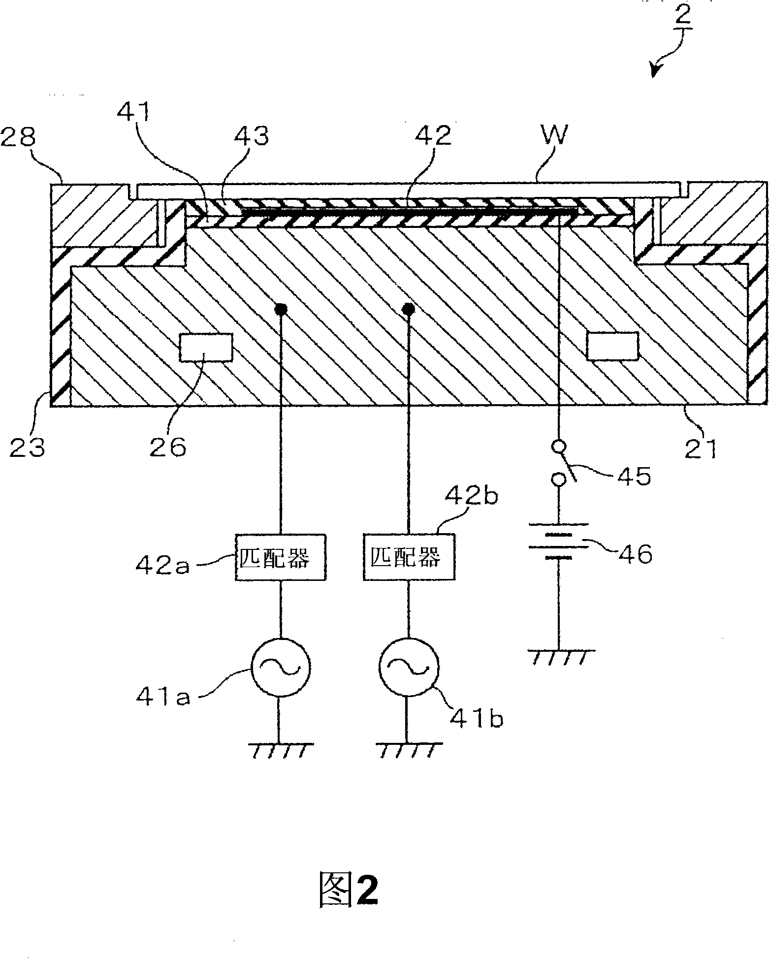
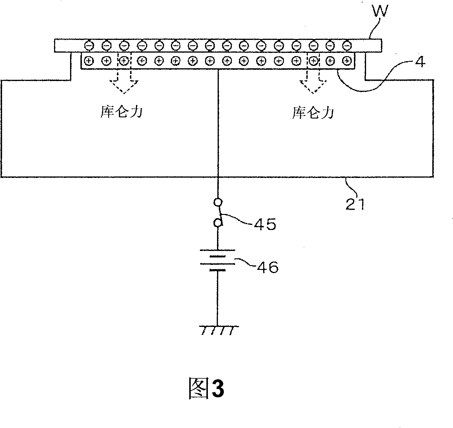
technical field [0001] The present invention relates to a mounting device provided with an electrostatic chuck layer that electrostatically adsorbs an object to be processed such as a semiconductor wafer, a plasma processing apparatus provided with the mounting device, and a plasma processing method. Background technique [0002] Mounting device used in a plasma processing device that performs plasma processing such as etching and CVD (Chemical Vapor Deposition), because a vacuum chuck cannot be used as a unit for holding a substrate on a mounting device , so use a general electrostatic chuck. [0003] An electrostatic chuck is placed on the surface of a carrier in a thin plate shape, a foil-shaped electrode is buried in an insulating layer, and the substrate is attracted to the electrostatic chuck by electrostatic force generated by applying, for example, a DC voltage to the electrode. function on the surface. [0004] When vacuum processing, such as plasma processing, is...
Claims
Login to View More Application Information
Patent Timeline
 Patent Type & Authority Applications(China)
IPC IPC(8): H01L21/683H01L21/67H01L21/3065H01L21/311H01L21/3213H01L21/02H01L21/00H01J37/32H05H1/00B08B7/00C23F4/00C23C16/44
CPCH01J37/32862H01L21/6833
Inventor 伊藤弘治加藤健一上田雄大
Owner TOKYO ELECTRON LTD
Features
- R&D
- Intellectual Property
- Life Sciences
- Materials
- Tech Scout
- Unparalleled Data Quality
- Higher Quality Content
- 60% Fewer Hallucinations
Learn More Browse by: Latest US Patents, China's latest patents, Technical Efficacy Thesaurus, Application Domain, Technology Topic, Popular Technical Reports.
© 2025 PatSnap. All rights reserved.Legal|Privacy policy|Modern Slavery Act Transparency Statement|Sitemap|About US| Contact US: help@patsnap.com