
IC label mounting structure and IC chip for installation

一种安装结构、安装用的技术,应用在机器使用的记录载体、印刷电路、仪器等方向,能够解决耐热性低、工件加热到高温限制、基材熔化等问题,达到容易制造、安装操作容易的效果

Inactive Publication Date: 2008-05-14
FUJITSU LTD
View PDF2 Cites 1 Cited by
  • Summary
  • Abstract
  • Description
  • Claims
  • Application Information

AI Technical Summary

Problems solved by technology

In particular, the IC chip used in recent IC tags is extremely small, so there is a problem that the work of combining the IC chip and the antenna board to manufacture the IC tag becomes complicated. We are looking for a method for mounting the IC chip on the antenna board more easily.
[0007] In addition, when the IC chip is connected to the antenna substrate by heating and pressurizing it with an adhesive, when the base material of the antenna substrate is made of a material with low heat resistance such as a polyethylene film, there is a possibility of heating. There is a problem that the base material melts when it reaches a high temperature, and there is also a problem that there is a limitation in heating the workpiece to a high temperature in terms of the manufacturing process.

Method used


Image

  • IC label mounting structure and IC chip for installation
  • IC label mounting structure and IC chip for installation
  • IC label mounting structure and IC chip for installation

Examples


no. 1 Embodiment approach

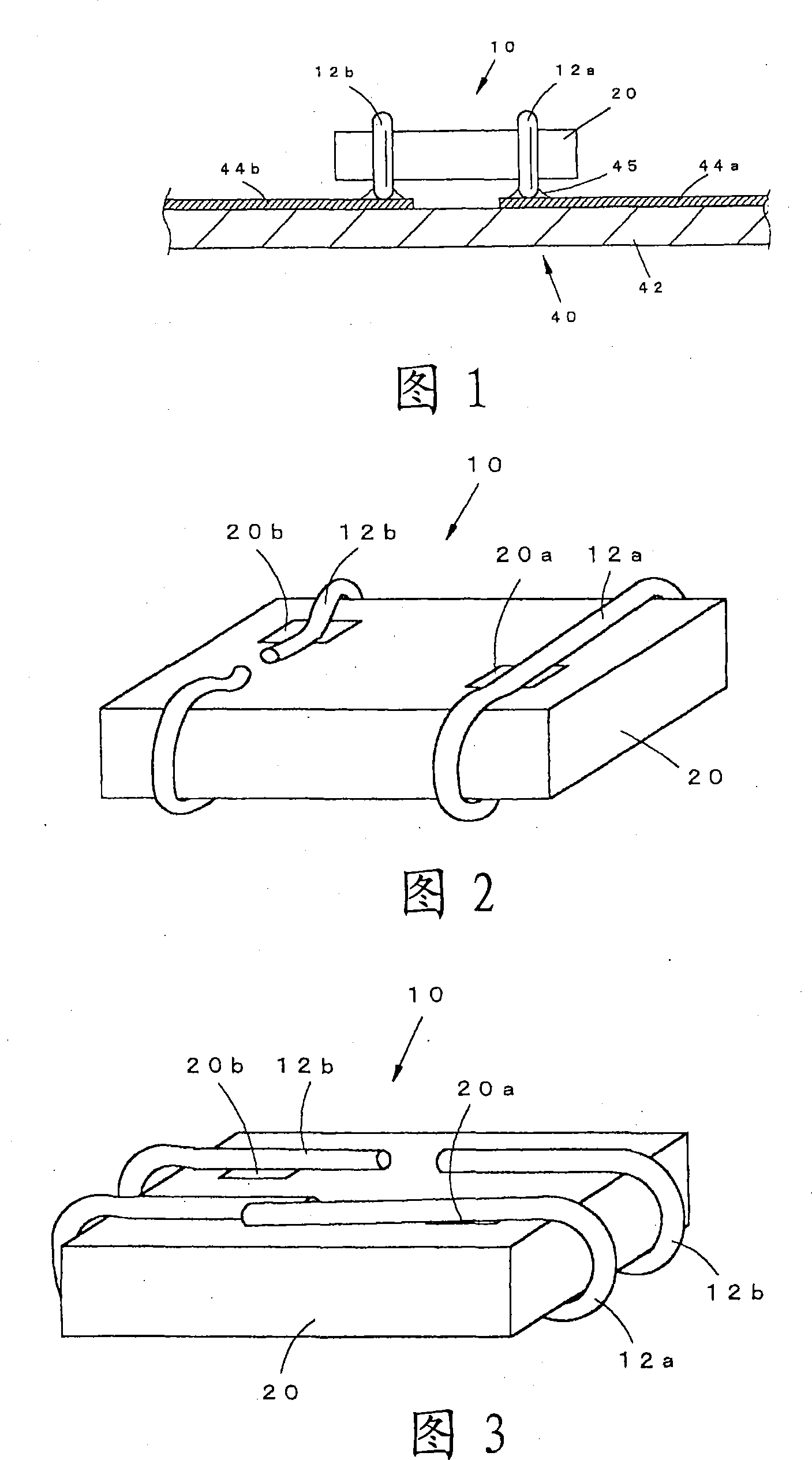
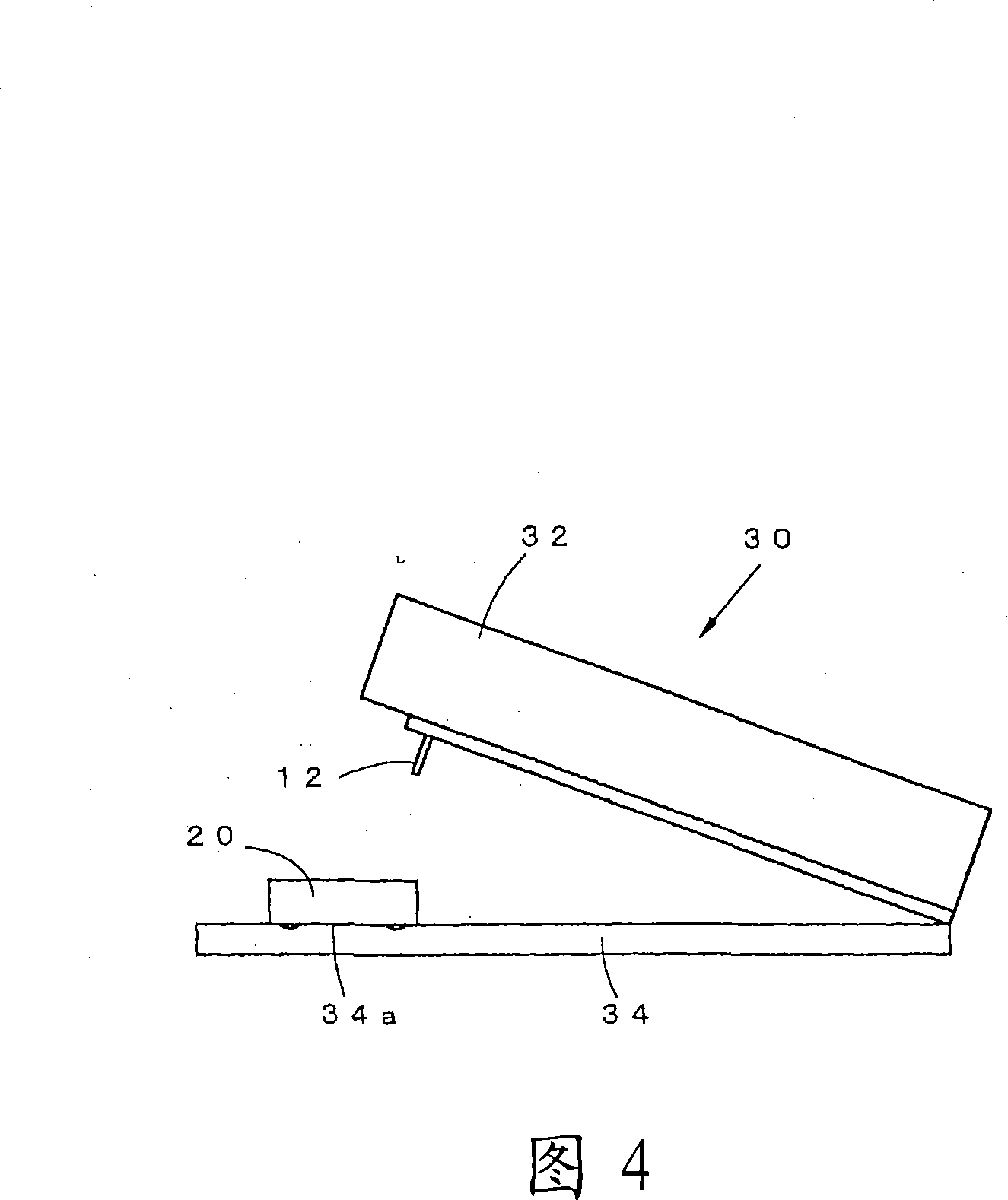
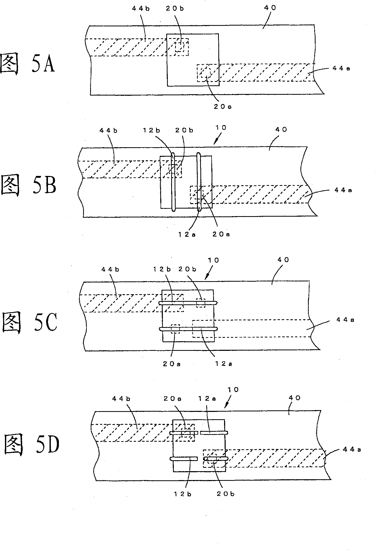
[0027] FIG. 1 is a cross-sectional view showing a first embodiment of a mounting structure of an IC tag according to the present invention. In the IC tag mounting structure of this embodiment, the IC chip 10 for mounting is electrically connected to the antenna patterns 44a and 44b formed on the front surface of the electrically insulating base film 42, and is mounted. The mounting IC chip 10 is formed by electrically connecting a pair of electrodes 20 a and 20 b formed on the IC chip 20 and winding conductive wires 12 a and 12 b around the outer surface of the IC chip 20 .

[0028] The mounting IC chip 10 is mounted on the antenna substrate 40 by connecting the conductive wires 12a, 12b wound and mounted on the IC chip 20 to the connection ends of the antenna patterns 44a, 44b with solder 45 . Thereby, the antenna patterns 44a, 44b and the IC chip 20 are electrically connected.

[0029] In addition, as a method of connecting the conductive wires 12a, 12b to the antenna patte...

no. 2 Embodiment approach

[0050] 6 is a cross-sectional view showing a second embodiment of the mounting structure of the IC tag according to the present invention. In the mounting structure of the IC tag of this embodiment, the IC chip 20 is positioned at the connection end of the antenna patterns 44a, 44b formed on the antenna substrate 40 so as to go around the outer surface of the IC chip 20 and the antenna substrate 40 together. The conductive wires 12 a and 12 b are wound in a form, and the IC chip 20 is mounted on the antenna substrate 40 .

[0051] FIG. 7 shows a winding device 35 for winding the conductive wire 12 together on the IC chip 20 and the antenna substrate 40, and the use of the winding device 35 to wind the conductive wire 12 on the IC chip 20 and the antenna substrate 40. method. The winding device 35 is formed in the same form as the stapler-shaped winding device 30 used when forming the above-mentioned IC chip 10 for mounting, and has a pressing part 36 which is accommodated in ...


PUM


Abstract

With a mounting structure for an IC tag where an IC chip for mounting (10) is mounted so as to be electrically connected to antenna patterns (44a), (44b), the assembly process that mounts the 1C chip for mounting (10) on the antenna patterns (44a), (44b) is simplified, which makes it possible to reduce the manufacturing cost of IC tags. The IC chip for mounting 10 is formed by winding conductive wires (12a), (12b) so as to encircle an outer surface of an IC chip (20) between two opposite edges of the IC chip (20) in a state where the conductive wires (12a), (12b) mechanically contact electrodes formed on the IC chip (20) and are electrically connected to the electrodes, so that the IC chip for mounting (10) is joined to the antenna patterns (44a), (44b) via the conductive wires (12a), (12b).

Description

technical field [0001] The present invention relates to a mounting structure of an IC tag formed by mounting an IC chip on an antenna substrate and an IC chip for mounting used therein. Background technique [0002] The IC tag is formed by mounting an IC chip on an antenna substrate on which an antenna for transmitting and receiving signals is formed. In the antenna substrate, an antenna pattern is formed on an electrically insulating film. The IC chip is mounted in a state where two electrodes provided on the chip are electrically connected to both ends of the antenna pattern, respectively. [0003] There are various methods for mounting an IC chip on an antenna substrate. For example, an adhesive is applied to an antenna substrate, and the electrodes of the IC chip and the terminals for connection of the antenna pattern are positioned, heated and pressurized, thereby An IC chip is bonded to the antenna substrate, and the antenna pattern and the IC chip are electrically c...

Claims


Application Information

Patent Timeline
Patent Type & Authority Applications(China)
IPC IPC(8): H01L21/60G06K19/07G06K19/077
CPCH01L24/48G06K19/07749H01L2224/4813H01L24/45H01L2224/48599H01L2924/01079H05K2201/10651H01L2924/14H01L2924/01005H01L2924/01033H05K2201/10386H01L2224/4809H01L2924/01029H05K3/3426H01L2224/45144H01L2224/4847H01L2224/48091H01L2924/014H05K2201/10636G06K19/0775H01L2224/48799H01L24/49H01L2224/45147H01L2224/49H01L2924/01047H01L2924/00014Y02P70/50H01L2924/00H01L2224/85399H01L2224/05599G06K19/077G06K19/07
Inventor 竹内周一
Owner FUJITSU LTD
Learn More