Technique for reducing silicide non-uniformities by adapting a vertical dopant profile

A material concentration, metal silicide technology, applied in semiconductor devices, electrical components, transistors, etc., can solve problems such as performance impact

Inactive Publication Date: 2008-06-04
ADVANCED MICRO DEVICES INC
View PDF0 Cites 2 Cited by
  • Summary
  • Abstract
  • Description
  • Claims
  • Application Information

AI Technical Summary

Problems solved by technology

Furthermore, as the drive to scale down semiconductor devices continues, the non-uniformity of the metal silicide region 117 may have a negative impact on the performance of next generation devices with tighter process tolerance settings

Method used


Image

  • Technique for reducing silicide non-uniformities by adapting a vertical dopant profile
  • Technique for reducing silicide non-uniformities by adapting a vertical dopant profile
  • Technique for reducing silicide non-uniformities by adapting a vertical dopant profile

Examples


Embodiment Construction

[0028] Exemplary specific embodiments of the present invention are described below. In the interest of clarity, this specification does not describe all features of an actual implementation. Of course, it should be understood that when developing any actual implementation, many implementation-related decisions must be made to achieve the developer's specific goals, such as compliance with system-related and business-related constraints, which will vary from implementation to implementation. . Furthermore, it should be appreciated that such development is complex and time consuming, yet is a matter of routine for those of ordinary skill in the art with the benefit of this disclosure.

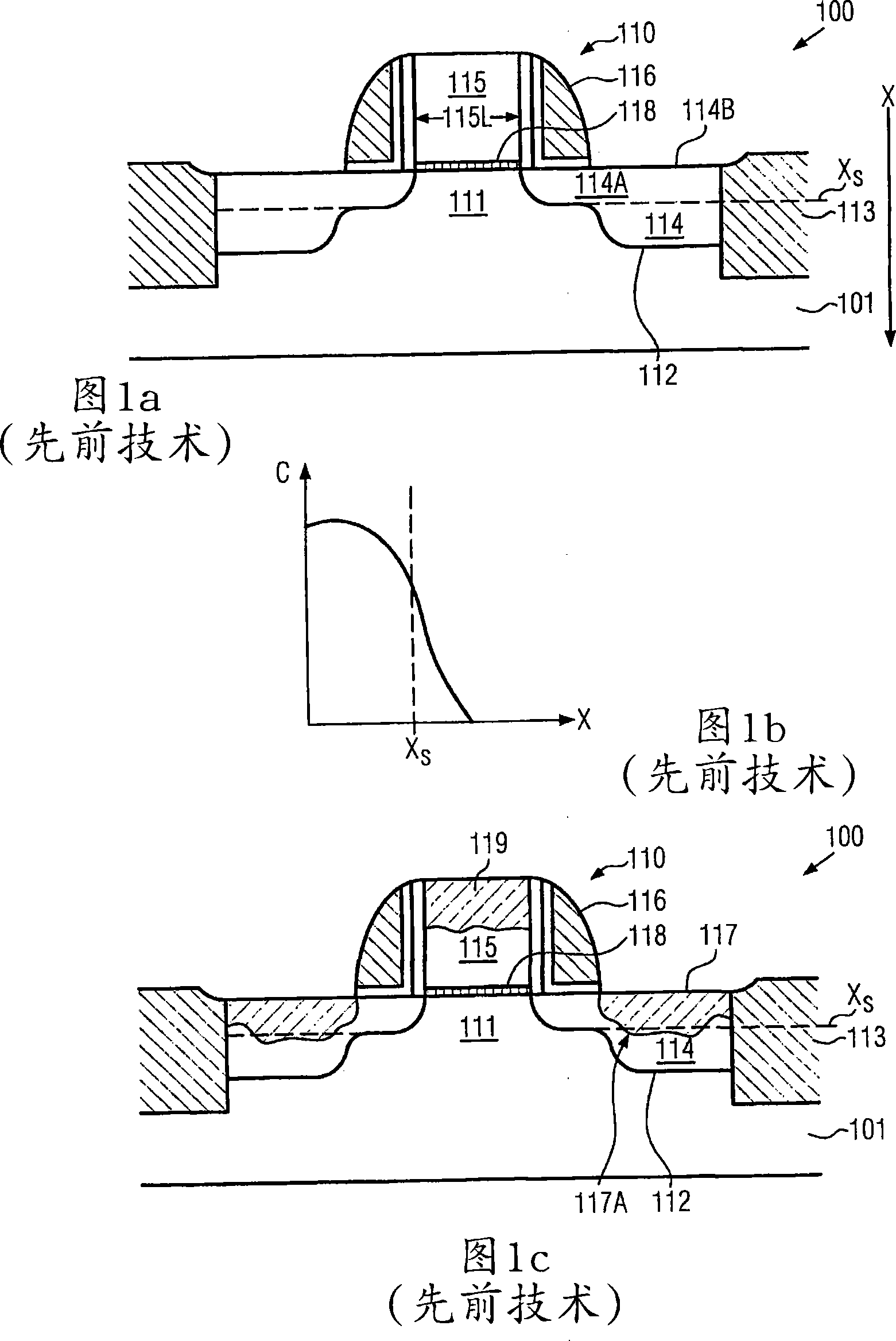
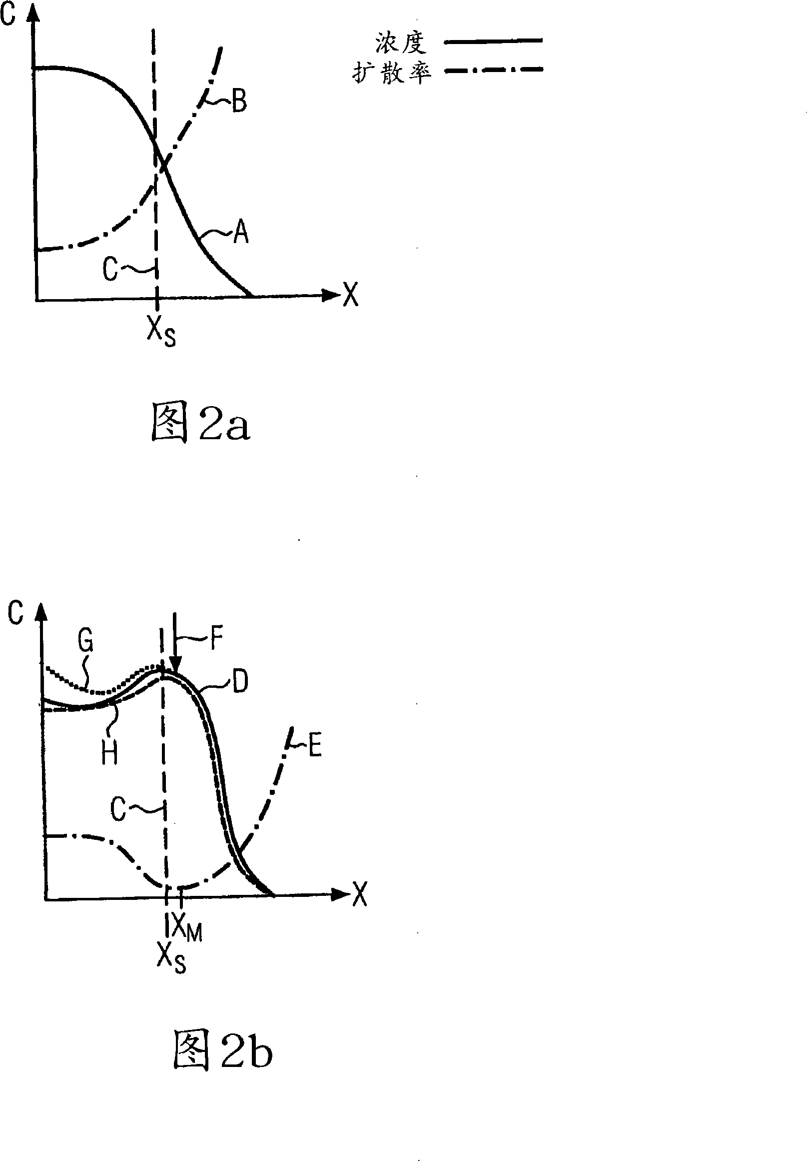
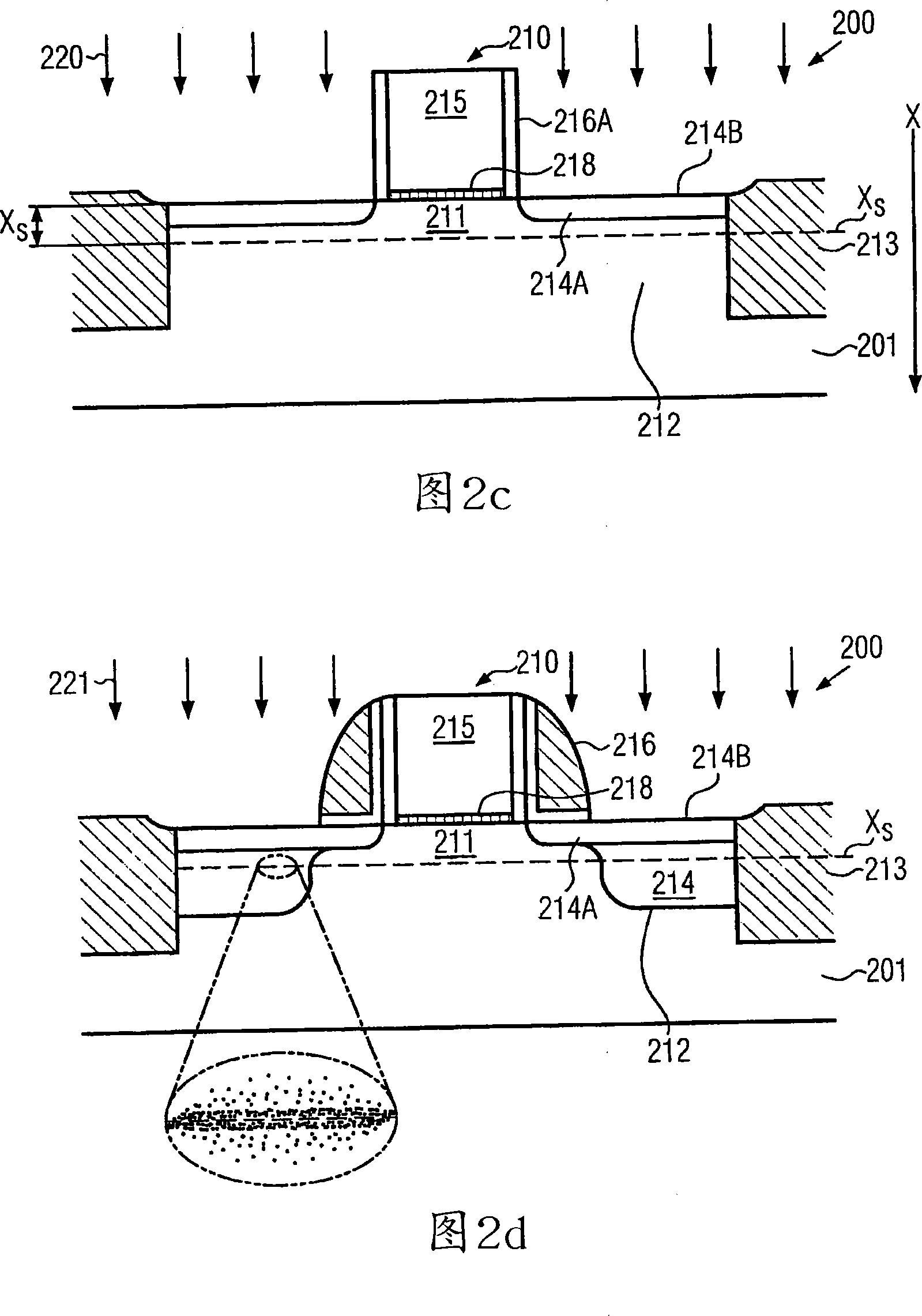
[0029] The present invention will now be described with reference to the accompanying drawings. Various structures, systems and devices are schematically illustrated in the drawings for purposes of explanation only and so that those skilled in the art will not be confused by details. Neverthel...


PUM


Abstract

By modifying the vertical dopant concentration in deep drain and source regions, the reaction behavior during the formation of metal silicide regions may be controlled. For this purpose, an increased dopant concentration is formed around a target depth for the metal silicide interface, thereby reducing the reaction speeds and thus improving the uniformity of the resulting metal silicide interface.

Description

technical field [0001] The present invention relates generally to the field of fabrication of integrated circuits, and more particularly to semiconductor devices having metal silicide portions on semiconductor regions to reduce the electrical resistance of said semiconductor regions. Background technique [0002] In modern ultra-high density integrated circuits, device features are steadily decreasing to enhance device performance and functionality. However, reducing feature size can cause problems that may partially negate the benefits gained through feature size reduction. In general, reducing the feature size of, for example, a transistor component results in a decrease in the channel resistance of the transistor component, resulting in a higher drive current capability and increased switching speed of the transistor. However, in reducing the feature size of these transistor devices, the resistance of the wires and contact regions (i.e., the regions connecting transistor...

Claims


Application Information

Patent Timeline
Patent Type & Authority Applications(China)
IPC IPC(8): H01L21/336H01L29/78
CPCH01L21/28518H01L21/823814H01L29/66507H01L29/6656H01L29/66628H01L21/26513H01L29/6659H01L29/4933
Inventor F·维尔博雷特D·布朗P·普雷斯
Owner ADVANCED MICRO DEVICES INC
Why Eureka
Try Eureka