Method and device for depositing film, deposited film and photosensitive body employing same
A technology for depositing films and controlling devices, which is applied in optics, gaseous chemical plating, coating, etc., can solve the problems of decreased film-forming speed, difficulty, and decreased reproducibility of deposited film characteristics, and achieves the reduction of film-forming speed, The effect of less uneven film thickness and uneven high-speed characteristics
- Summary
- Abstract
- Description
- Claims
- Application Information
AI Technical Summary
Problems solved by technology
Method used
Image

Examples
Embodiment 1
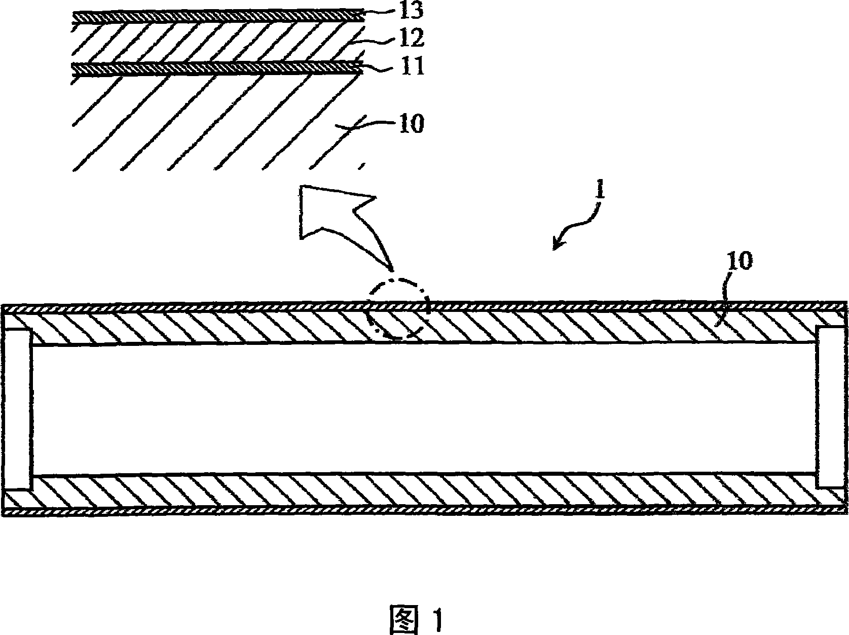
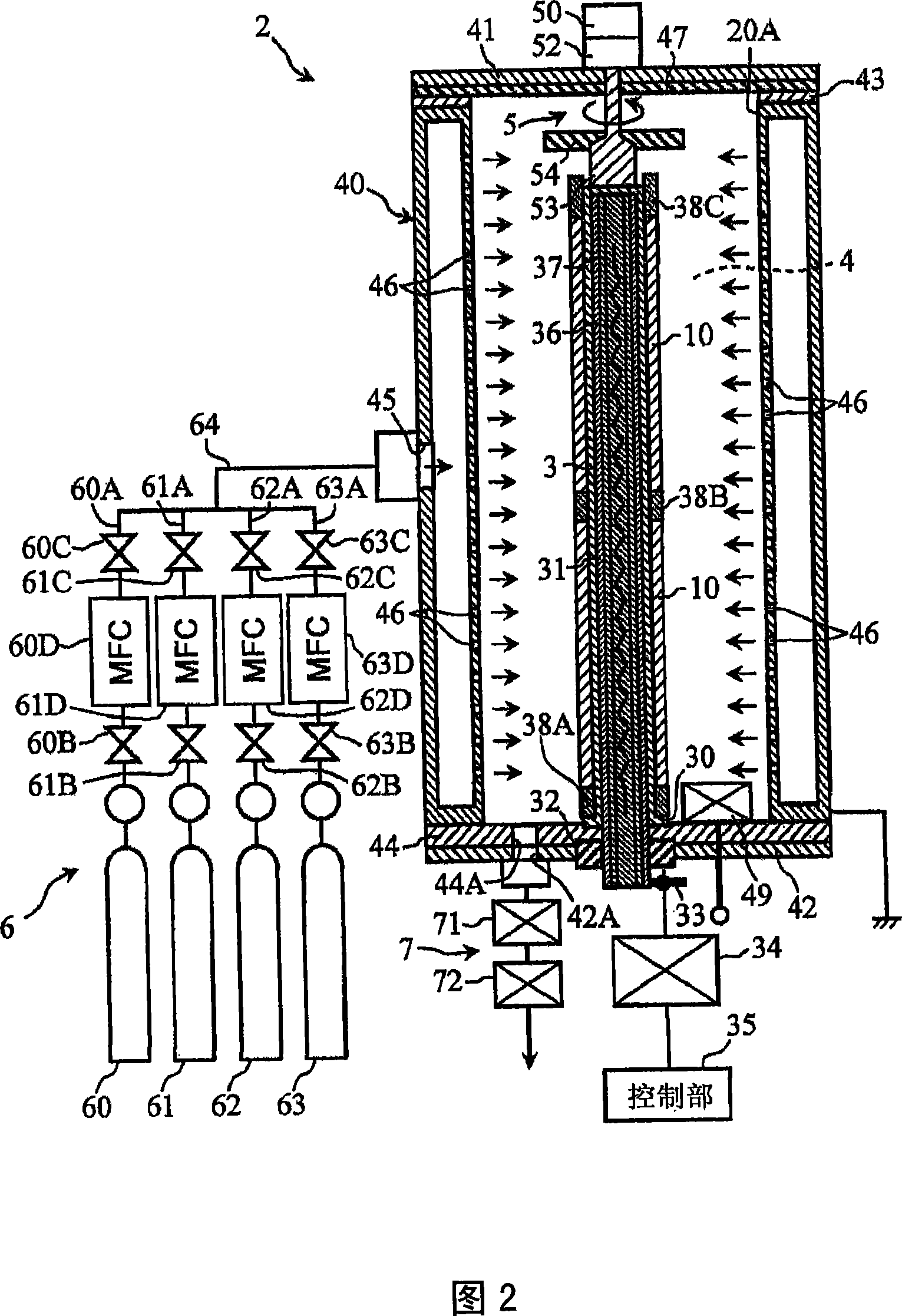
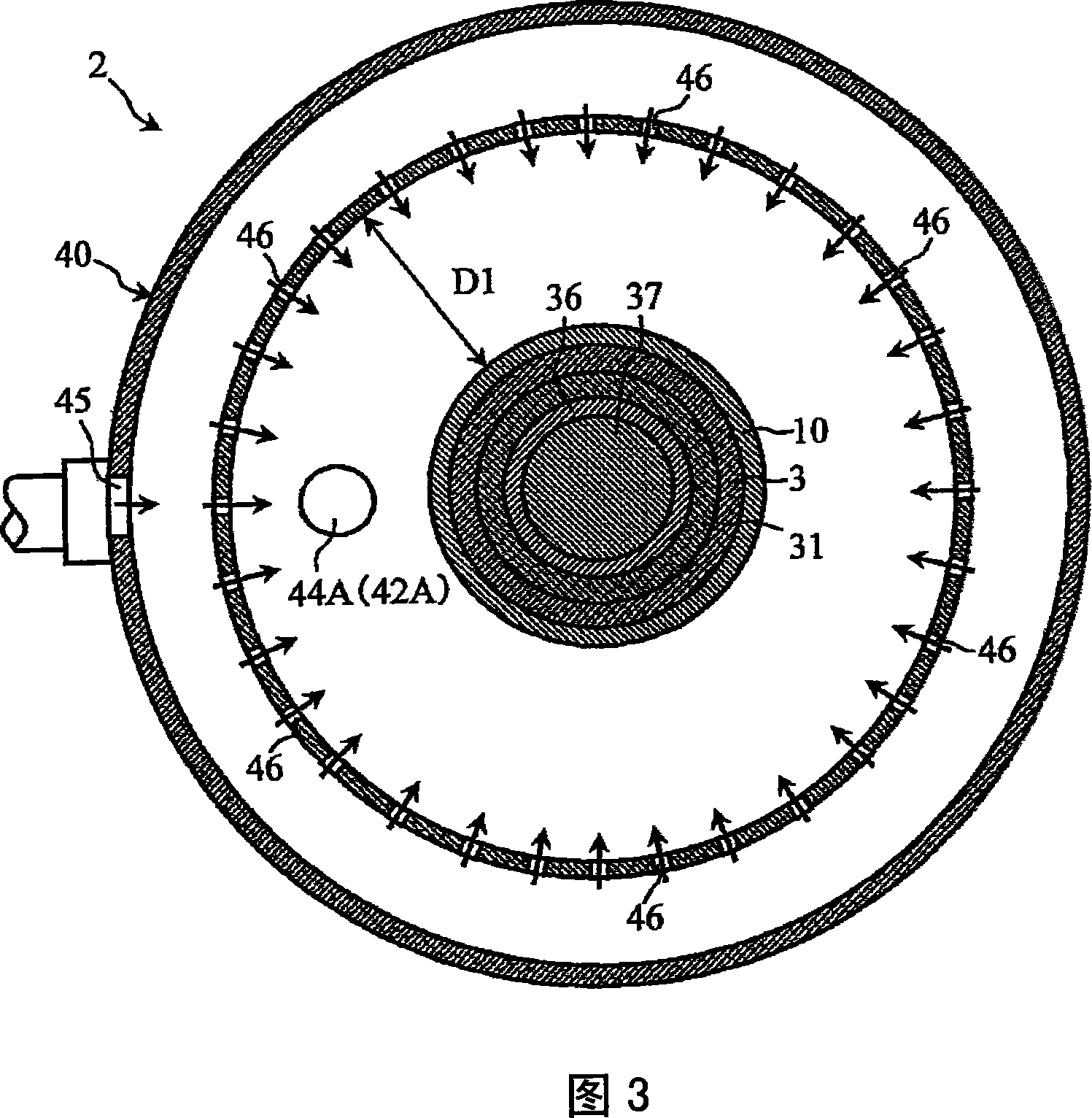
[0140] In this embodiment, a negative pulsed direct current voltage is applied between the cylindrical substrate 10 (support body 3) and the cylindrical electrode 40 using the plasma CVD apparatus 2 shown in FIGS. 2 to 4 (see FIG. 5) The influence of the frequency and voltage value of the pulsed direct current voltage on the frequency of occurrence of arc discharge (abnormal discharge) was studied during film formation.
[0141] In the plasma CVD apparatus 2, the distance D1 between the cylindrical substrate 10 and the cylindrical electrode 40 was set to 25 mm, and film formation conditions other than the applied voltage were as shown in Table 1 below.
[0142] [Table 1]
[0143]
raw gas
SiH 4 (sccm)
340
h 2 (sccm)
200
B 2 h 6 (ppm)
0
CH 4 (sccm)
0
Pressure (Pa)
60
Substrate temperature (°C)
320
[0144] Negative pulsed DC voltage was a...
Embodiment 2
[0153] In this embodiment, the film is formed by applying a negative pulsed DC voltage between the cylindrical substrate 10 (support body 3 ) and the cylindrical electrode 40 using the plasma CVD apparatus 2 shown in FIGS. 2 to 4 . , the influence of the duty ratio of the pulsed DC voltage on the number of occurrences of arc discharge (abnormal discharge) was studied.
[0154] The duty cycle of the pulsed DC voltage was set in the range of 10% to 95%, and the frequency and voltage value of the pulsed DC voltage were set to 30 kHz and −1000 V, respectively. Film formation conditions other than the applied voltage were the same as in Example 1.
[0155] The number of occurrences of arc discharge during film formation is shown in Table 3 below. In addition, in Table 3, the number of occurrences of arc discharge is shown in the number of occurrences per hour.
[0156] [table 3]
[0157] Frequency 300kHz, potential difference -1000V
[0158] Duty cycle (%)
10
...
Embodiment 3
[0162] In this embodiment, the film is formed by applying a negative pulsed DC voltage between the cylindrical substrate 10 (support body 3 ) and the cylindrical electrode 40 using the plasma CVD apparatus 2 shown in FIGS. 2 to 4 . , the influence of the voltage value of the pulsed DC voltage (the potential difference between the cylindrical electrode 40 and the cylindrical substrate 10 (support 3 )) on the film formation rate was investigated.
[0163] The voltage value of the pulsed DC voltage is set in the range of 10V-4000V, and the frequency and duty cycle of the pulsed DC voltage are set to 30kHz and 50%, respectively. Film formation conditions other than the applied voltage were the same as in Example 1. The results of the measurement of the film formation rate are shown in FIG. 9 .
[0164] As shown in FIG. 9 , the larger the voltage value (-V) of the negative pulse-shaped DC voltage, the higher the film formation rate. Therefore, when applying a negative pulse-shape...
PUM
| Property | Measurement | Unit |
|---|---|---|
| thickness | aaaaa | aaaaa |
| thickness | aaaaa | aaaaa |
| thickness | aaaaa | aaaaa |
Abstract
Description
Claims
Application Information
 - R&D
- Intellectual Property
- Life Sciences
- Materials
- Tech Scout
- Unparalleled Data Quality
- Higher Quality Content
- 60% Fewer Hallucinations
Browse by: Latest US Patents, China's latest patents, Technical Efficacy Thesaurus, Application Domain, Technology Topic, Popular Technical Reports.
© 2025 PatSnap. All rights reserved.Legal|Privacy policy|Modern Slavery Act Transparency Statement|Sitemap|About US| Contact US: help@patsnap.com