Method and device for manufacturing photosensitive body
一种制造方法、感光体的技术,应用在光学、仪器、涂层等方向,能够解决困难、沉积膜成膜速度下降等问题,达到膜厚不均少、成膜速度抑制、膜厚不均优质的效果
- Summary
- Abstract
- Description
- Claims
- Application Information
AI Technical Summary
Problems solved by technology
Method used
Image

Examples
Embodiment 1
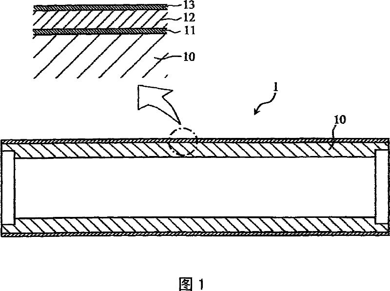
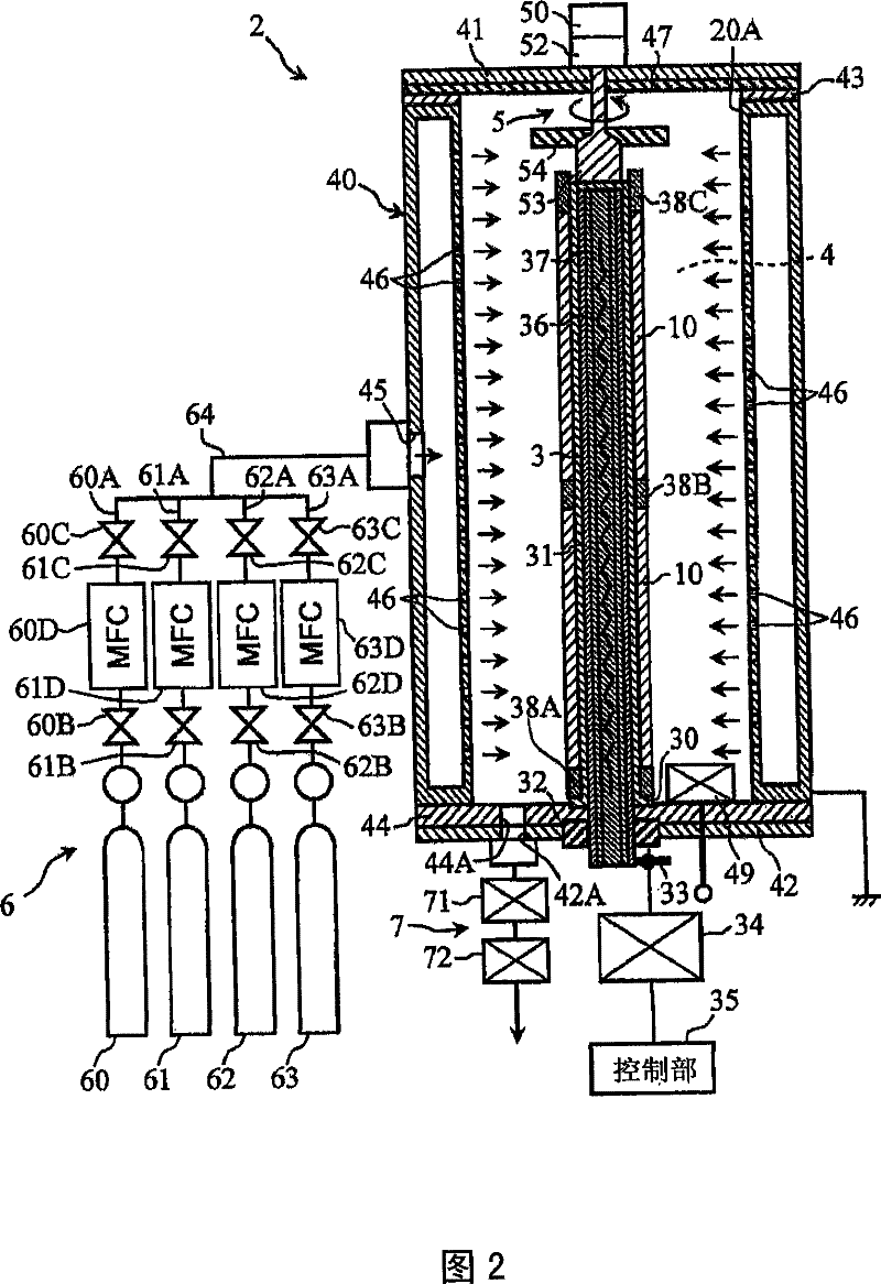
[0143] In this example, using Figure 2 ~ Figure 4 In the shown plasma CVD apparatus 2, a negative pulsed DC voltage is applied between the cylindrical substrate 10 (support 3) and the cylindrical electrode 40 (refer to Figure 5 ) to form a film, the influence of the frequency and voltage value of the pulsed DC voltage on the frequency of arc discharge (abnormal discharge) was studied.
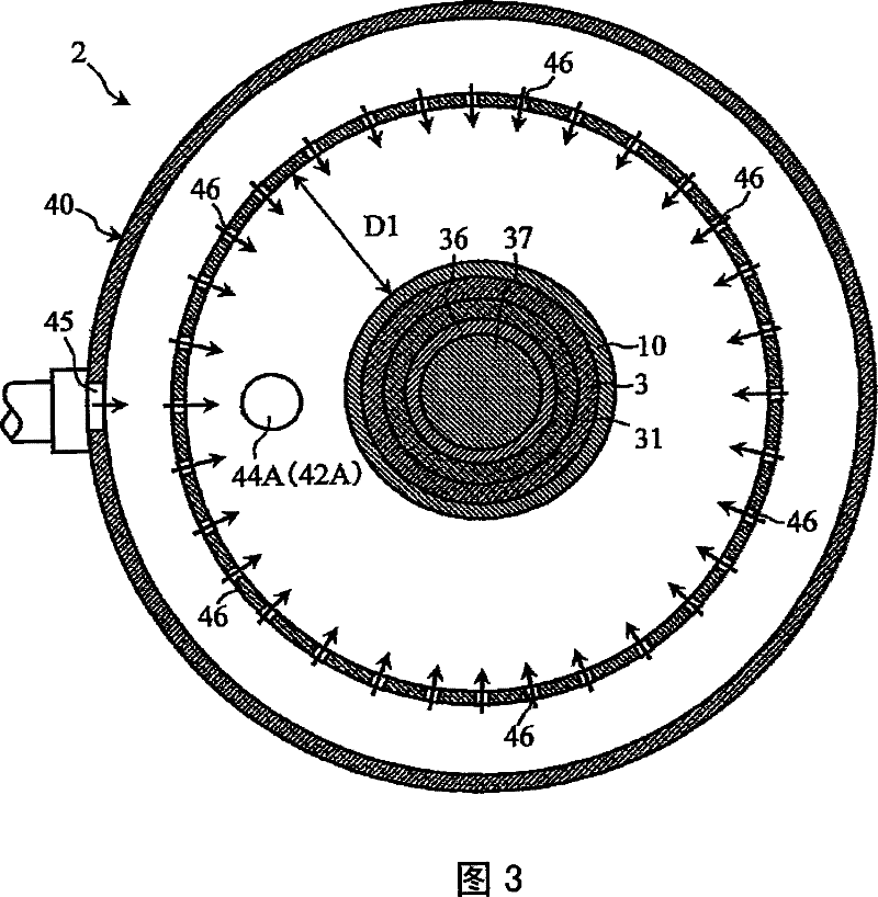
[0144] In the plasma CVD apparatus 2, the distance D1 between the cylindrical substrate 10 and the cylindrical electrode 40 was set to 25 mm, and film formation conditions other than the applied voltage were as shown in Table 1 below.
[0145] [Table 1]
[0146]
[0147] Negative pulsed DC voltage was applied by supplying a pulsed voltage in the range of -4000V to -10V from a DC power supply 34 connected to the cylindrical base 10 (support 3 ), while grounding the cylindrical electrode 40 . The frequency of the negative pulse-shaped DC voltage is set in the range of 10 kHz to 500 kHz. ...
Embodiment 2
[0156] In this example, using Figure 2 ~ Figure 4 In the shown plasma CVD apparatus 2, when a negative pulsed DC voltage is applied between the cylindrical substrate 10 (support 3) and the cylindrical electrode 40 to form a film, the duty ratio of the pulsed DC voltage is studied. The influence of the frequency of occurrence of arc discharge (abnormal discharge).
[0157] The duty cycle of the pulsed DC voltage was set in the range of 10% to 95%, and the frequency and voltage value of the pulsed DC voltage were set to 30 kHz and −1000 V, respectively. Film formation conditions other than the applied voltage were the same as in Example 1.
[0158] The number of occurrences of arc discharge during film formation is shown in Table 3 below. In addition, in Table 3, the number of occurrences of arc discharge is shown in the number of occurrences per hour.
[0159] [table 3]
[0160] Frequency 300kHz, potential difference -1000V
[0161]
[0162] ×: Unstable discharge
[...
Embodiment 3
[0165] In this example, using Figure 2 ~ Figure 4 In the plasma CVD apparatus 2 shown, when a negative pulsed DC voltage is applied between the cylindrical substrate 10 (support 3) and the cylindrical electrode 40 to form a film, the voltage value of the pulsed DC voltage (circular The influence of the potential difference between the cylindrical electrode 40 and the cylindrical base 10 (support 3 )) on the film formation rate.
[0166] The voltage value of the pulsed DC voltage is set in the range of 10V-4000V, and the frequency and duty cycle of the pulsed DC voltage are set to 30kHz and 50%, respectively. Film formation conditions other than the applied voltage were the same as in Example 1. The results of the measurement of the film forming speed are as follows: Figure 9 shown.
[0167] Such as Figure 9 It was shown that the larger the voltage value (-V) of the negative pulse-shaped DC voltage, the higher the film formation rate. Therefore, when applying a negative...
PUM
| Property | Measurement | Unit |
|---|---|---|
| aperture size | aaaaa | aaaaa |
| coefficient of thermal expansion | aaaaa | aaaaa |
| diameter | aaaaa | aaaaa |
Abstract
Description
Claims
Application Information
 - R&D
- Intellectual Property
- Life Sciences
- Materials
- Tech Scout
- Unparalleled Data Quality
- Higher Quality Content
- 60% Fewer Hallucinations
Browse by: Latest US Patents, China's latest patents, Technical Efficacy Thesaurus, Application Domain, Technology Topic, Popular Technical Reports.
© 2025 PatSnap. All rights reserved.Legal|Privacy policy|Modern Slavery Act Transparency Statement|Sitemap|About US| Contact US: help@patsnap.com