Electronic device and method of manufacturing the same

A technology of electronic devices and conductive layers, applied in the field of electronic devices and their manufacturing, to achieve the effects of reduced process operations, simple structure, and reduced process operations

Active Publication Date: 2008-06-18
SAMSUNG DISPLAY CO LTD
View PDF1 Cites 36 Cited by
  • Summary
  • Abstract
  • Description
  • Claims
  • Application Information

AI Technical Summary

Problems solved by technology

[0004] According to the current state of the art, there is no convenient method for directly patterning insulating materials such as fluorinated organic polymers

Method used


Image

  • Electronic device and method of manufacturing the same
  • Electronic device and method of manufacturing the same
  • Electronic device and method of manufacturing the same

Examples


Embodiment Construction

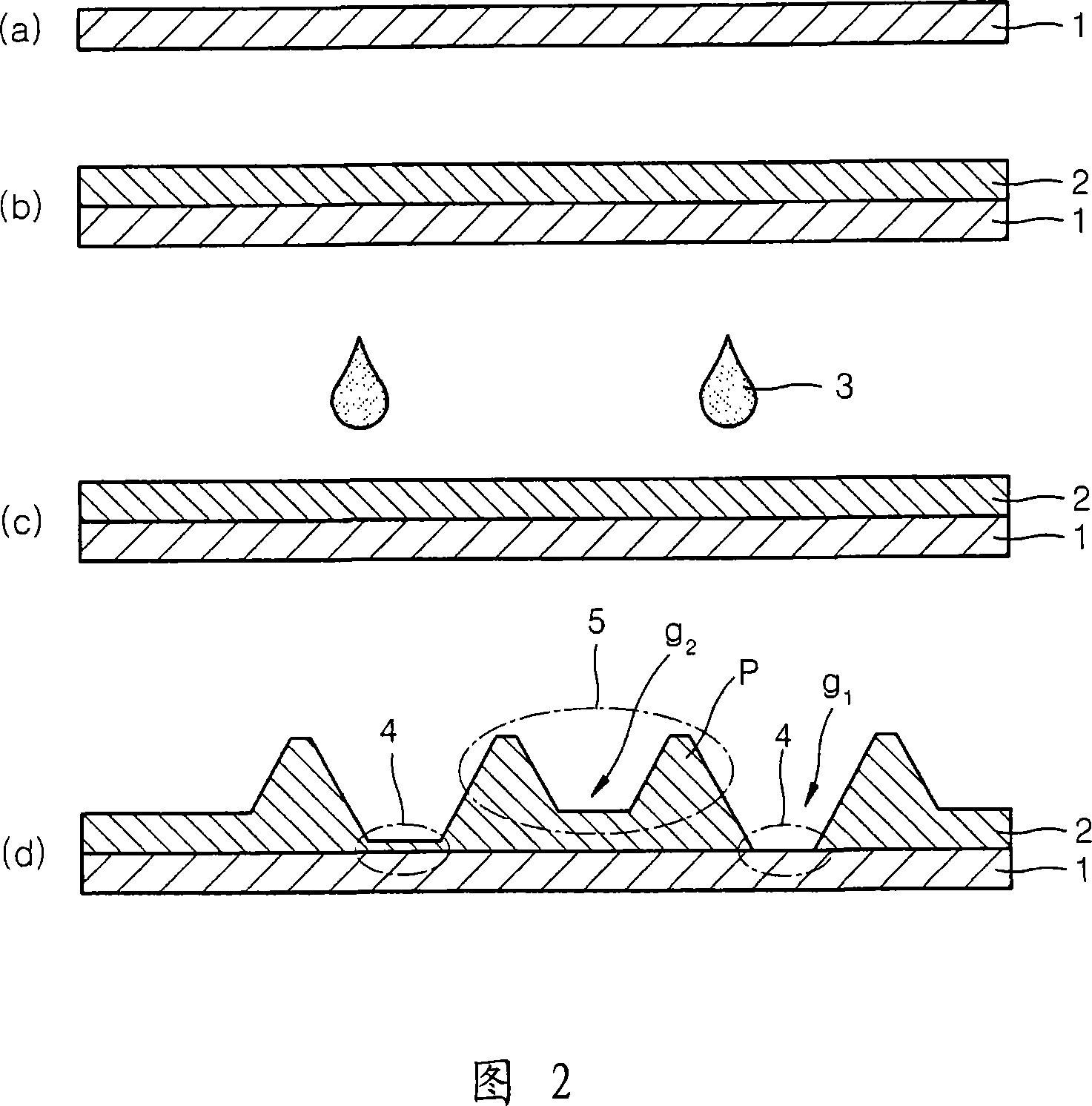
[0048] Certain embodiments are described more fully hereinafter with reference to the accompanying drawings, which illustrate exemplary embodiments. In general, it should be noted that, for the sake of clarity, a reference number has not been attached to every element in every figure, but rather the reference number is only listed the first time an element is shown. Therefore, it should be understood that elements with the same hatching represent elements with the same function.

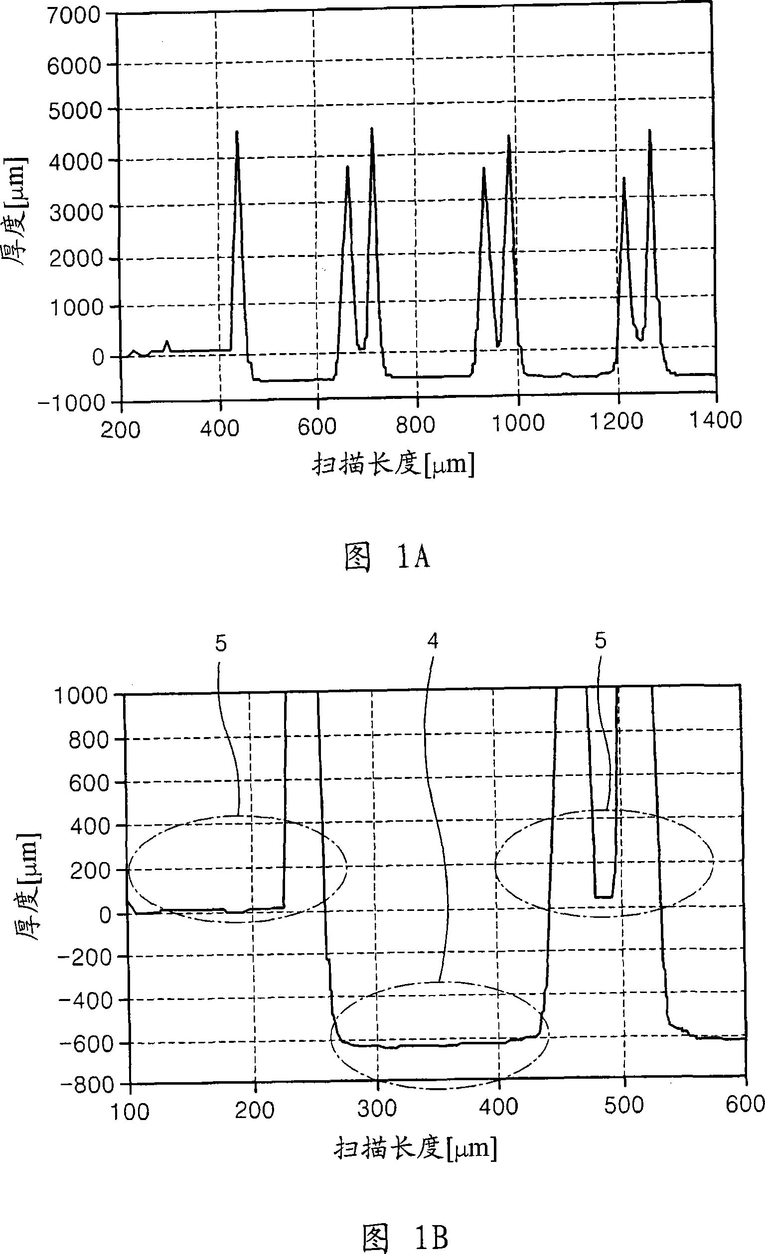
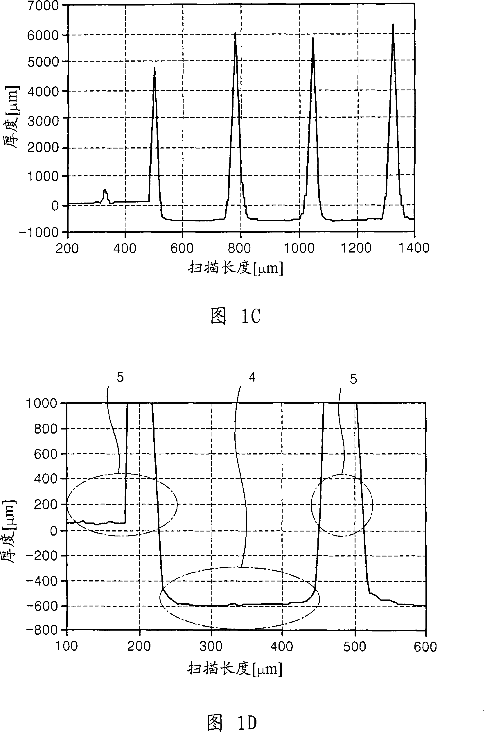
[0049] 1A-1D are cross-sectional views of embodiments of on-substrate bank structures used in the fabrication of organic light emitting diodes (OLEDs). In FIGS. 1A-1D , the unit of the horizontal axis is μm, and the unit of the vertical axis is μm.

[0050] Figure 1A shows a cross-sectional view of an embodiment of a bank structure that can be used to fabricate a substrate of an OLED. FIG. 1B shows an enlarged view of the bank structure of the substrate of FIG. 1A. In order to obtain a substrate hav...


PUM


Abstract

Provided are an electronic device including a bank structure and a manufacturing method thereof. Methods of fabricating electronic devices require a relatively small number of steps and include the possibility of direct patterning of insulating layers such as fluorinated organic polymer layers using cost-effective techniques such as inkjet printing.

Description

[0001] Cross References to Related Applications [0002] This application claims priority from European Patent Application No. 06126004.8 filed on December 13, 2006 and Korean Patent Application No. 10-2007-0036180 filed on April 12, 2007, the disclosures of which are incorporated herein by reference in their entirety. technical field [0003] The present disclosure mainly relates to an electronic device and a manufacturing method thereof, and more particularly to an organic light emitting diode including a bank structure and a manufacturing method thereof; It further relates to a method for forming a gate electrode of a thin film transistor (TFT) of an organic light emitting diode (OLED) and an electrophoretic device. Background technique [0004] According to the current state of the art, there is no convenient method for directly patterning insulating materials such as fluorinated organic polymers. The term "insulating material" as used herein is understood as a material...

Claims


Application Information

Patent Timeline
Patent Type & Authority Applications(China)
IPC IPC(8): H01L51/00H01L51/40H01L51/56H01L51/10H01L51/52H01L21/00H01L27/32
CPCH01L27/3244H01L51/0019H10K59/12H10K71/236H05B33/22H05B33/10
Inventor 阿瑟·玛西娅乔尔格·费希尔马库斯·谢迪格
Owner SAMSUNG DISPLAY CO LTD
Why Eureka
Try Eureka