Method for fabricating image sensor

An image sensor and pattern technology, which is used in semiconductor/solid-state device manufacturing, instruments, electrical solid-state devices, etc., can solve the problems of reducing the sensitivity of image sensors, reducing manufacturing output, etc., to improve sensitivity, reduce size, and reduce light convergence. effect of distance

Inactive Publication Date: 2008-07-02
DONGBU HITEK CO LTD
View PDF0 Cites 7 Cited by
  • Summary
  • Abstract
  • Description
  • Claims
  • Application Information

AI Technical Summary

Problems solved by technology

Particles on the microlens not only reduce the sensitivity of the image sensor, but also reduce the manufacturing yield due to the difficulty of cleaning the microlens

Method used


Image

  • Method for fabricating image sensor
  • Method for fabricating image sensor
  • Method for fabricating image sensor

Examples


Embodiment Construction

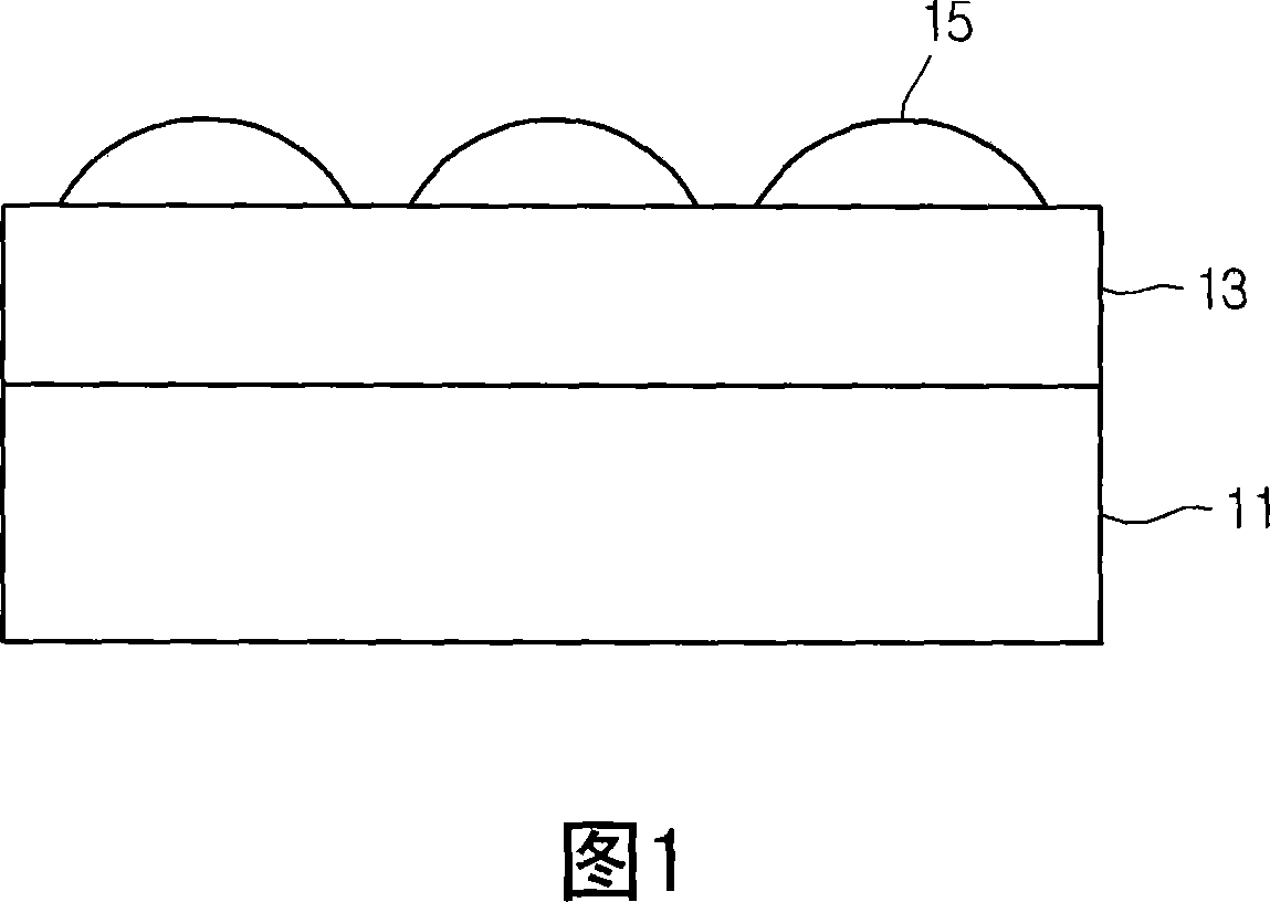
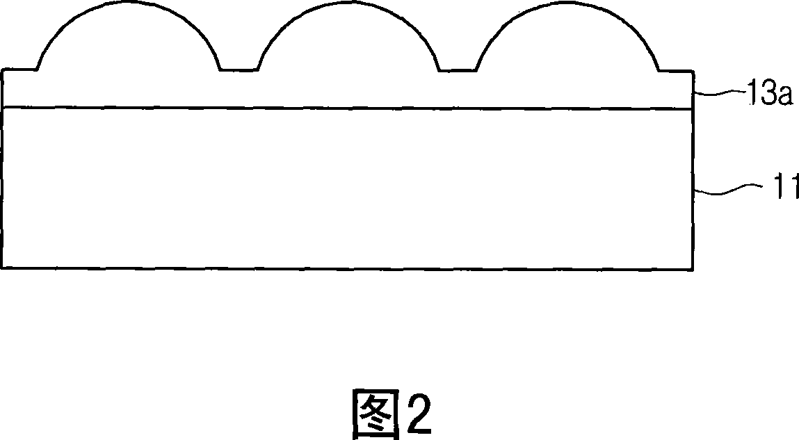
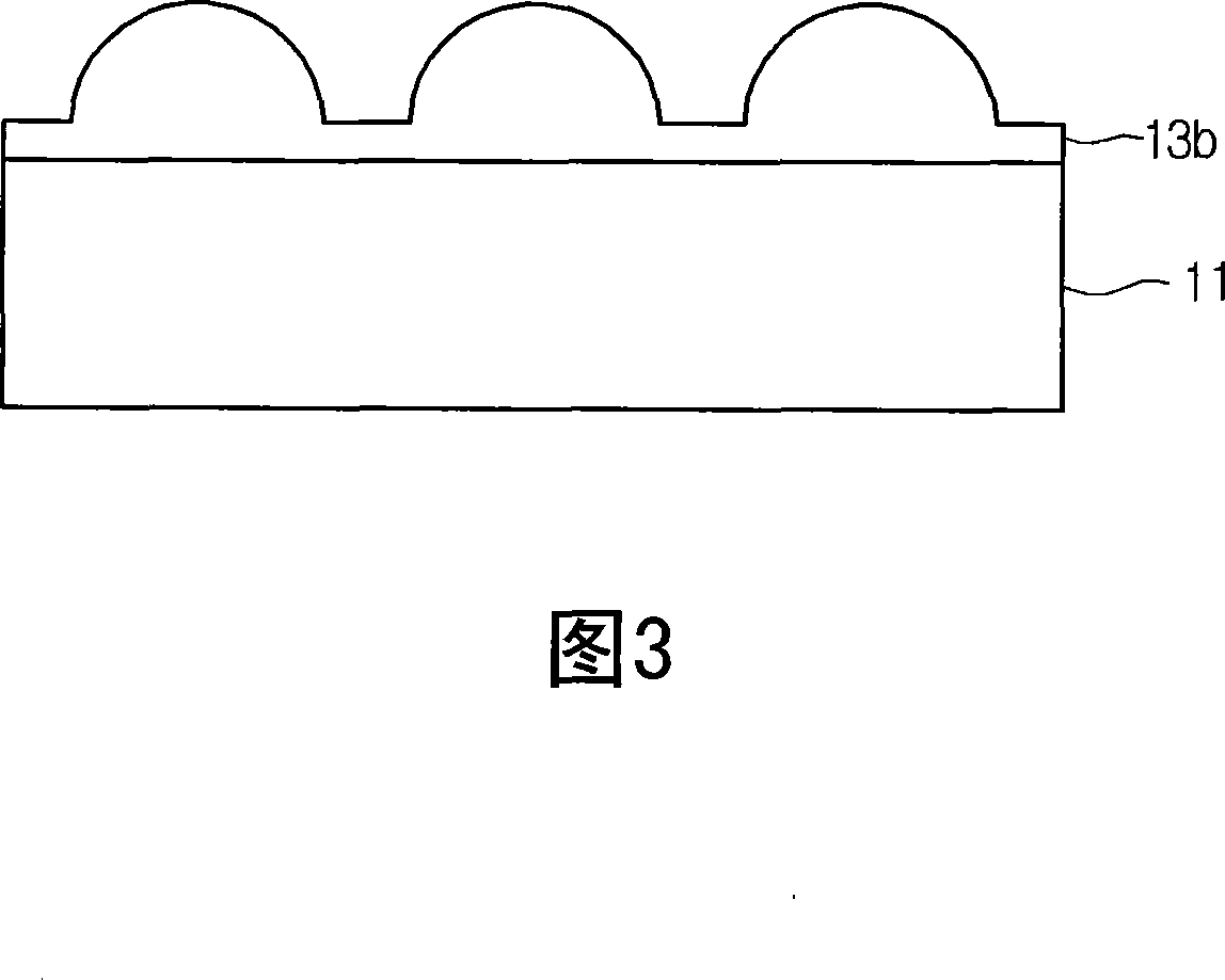
[0015] In the description of the embodiments of the present invention, it should be understood that when a layer (or film), region, pattern or structure refers to another substrate, another layer (or film), another region, another When "on / over" or "under / under" a liner or another pattern, it may be directly on the other substrate, layer (or film), region, liner or pattern, or intervening layers may also be present. Furthermore, it should be understood that when a layer (or film), region, pattern, liner or structure is referred to as being "between" two layers (or films), region, liner or pattern, it is meant that it There may be only one layer between two layers (or films), two regions, pads or patterns, or one or more intervening layers may also be present. Therefore, this should be determined by the technical concept of the present invention.

[0016] Hereinafter, embodiments of the present invention will be described in detail with reference to the accompanying drawings. ...


PUM


Abstract

The present invention provides a method of manufacturing an image sensor. In this method, a low temperature oxide layer is formed on the color filter layer, and a photoresist pattern is formed on the low temperature oxide layer. Subsequently, heat treatment is performed on the photoresist pattern to form sacrificial microlenses. The sacrificial microlenses and the low temperature oxide layer are etched to form preliminary microlenses in the low temperature oxide layer. The preliminary microlenses are etched to form microlenses having a reduced radius of curvature compared to the preliminary microlenses. According to the method of manufacturing an image sensor of the present invention, the sensitivity of the image sensor is improved, and the light convergence distance is reduced, so that the size of the image sensor can be reduced.

Description

technical field [0001] The invention relates to an image sensor and a manufacturing method thereof. Background technique [0002] Image sensors are semiconductor devices that convert optical images into electrical signals. One of the difficulties to be solved in manufacturing an image sensor is to increase the rate at which an incident light signal is converted into an electrical signal (ie, sensitivity). [0003] Various methods have been proposed in forming microlenses for converging light to realize a zero gap such that no gap is created between adjacent microlenses for forming a microlens array. [0004] When photoresists are used to form microlenses, particles such as polymers may attach to the microlenses during wafer backgrinding and sawing processes. Particles on the microlens not only reduce the sensitivity of the image sensor, but also reduce the manufacturing yield due to the difficulty of cleaning the microlens. Accordingly, various methods of forming microlen...

Claims


Application Information

Patent Timeline
Patent Type & Authority Applications(China)
IPC IPC(8): H01L21/71H01L21/82H01L27/146
CPCB29D11/00365G02B3/0018H01L27/14627H01L27/14685H01L27/146
Inventor 尹基准黃祥逸
Owner DONGBU HITEK CO LTD
Why Eureka
Try Eureka