Pixel structure and its making method

A pixel structure and manufacturing method technology, which is applied in semiconductor/solid-state device manufacturing, optics, instruments, etc., can solve the problems of high cost, complex manufacturing of reflective pixel electrodes and photoresist bumps, etc., and achieve the effect of improving reflectivity

Active Publication Date: 2010-06-16
AU OPTRONICS CORP
View PDF8 Cites 0 Cited by
  • Summary
  • Abstract
  • Description
  • Claims
  • Application Information

AI Technical Summary

Problems solved by technology

However, the pad layer, reflective pixel electrodes on the pad layer, and photoresist bumps are complex and costly to manufacture.

Method used


Image

  • Pixel structure and its making method
  • Pixel structure and its making method
  • Pixel structure and its making method

Examples


Embodiment Construction

[0053] In order to make the above-mentioned features and advantages of the present invention more comprehensible, preferred embodiments will be described in detail below together with the accompanying drawings.

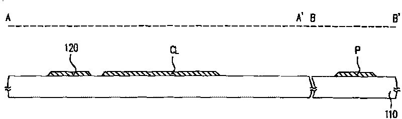
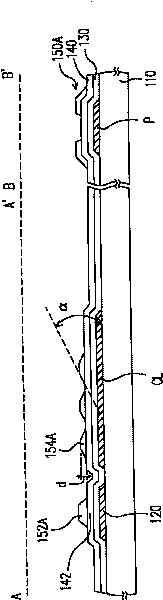
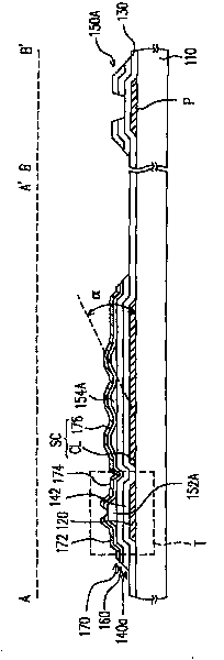
[0054] Generally speaking, disposing reflective pixel electrodes in the pixel structure can make the pixel structure have the ability to reflect light. It has both transmissive and reflective display modes. It can be seen from the description of the prior art that in order to make this type of pixel structure have good quality, a pad layer for padding the reflective pixel electrode and a photoresist bump to improve the reflectivity are usually made in the pixel structure, but this method will lead to The manufacturing process of the pixel structure becomes complicated, which reduces the output and product yield. Therefore, the present invention proposes a method for manufacturing a pixel structure, so as to manufacture a pixel structure with good quality under the pr...


PUM

PropertyMeasurementUnit
thicknessaaaaaaaaaa
thicknessaaaaaaaaaa

Abstract

The invention relates to a pixel structure and the manufacturing method, the pixel structure includes a grid, a grid layer, a patterning semiconductor layer which is provided with a channel area abovethe grid, a patterning dielectric layer which includes an etch stop layer above the grid and a plurality of convex blocks, a patterning metal layer which includes a reflection pixel electrode, a source and a drain which respectively cover part area of the channel area, a flattening dielectric layer and a transparent pixel electrode, and the components are sequentially arranged on a base plate. The reflection pixel electrode is connected with the drain and covers the convex blocks so as to form a concave and convex surface. The flattening dielectric layer is arranged on a transistor which is composed of the grid, the grid dielectric layer, the patterning semiconductor layer, the source and the drain; furthermore, the invention is provided with a contact window to expose part area of the reflection pixel electrode. The transparent pixel electrode is electrically connected with the reflection pixel electrode by the contact window.

Description

technical field [0001] The present invention relates to a pixel structure and manufacturing method thereof, and in particular to a pixel structure with a reflective electrode (reflective electrode) and a manufacturing method thereof. Background technique [0002] With the popularization of liquid crystal displays (LCDs), many portable electronic devices (portable electronic devices) have gradually increased requirements for the display functions of liquid crystal displays, especially portable electronic products such as mobile phones ( mobile phone), personal digital assistant (personal digital assistant, PDA) or palmtop computer (pocket PC), etc. These portable electronic products not only need to have a good picture display effect indoors, but also need to maintain an appropriate picture quality outdoors or under strong light conditions. [0003] Therefore, how to maintain a good display quality of the liquid crystal display in a strong light environment has become one of...

Claims


Application Information

Patent Timeline
Patent Type & Authority Patents(China)
IPC IPC(8): H01L27/12H01L23/522H01L21/84H01L21/768G02F1/1362
Inventor 林祥麟曹俊杰
Owner AU OPTRONICS CORP
Why Eureka
Try Eureka