
Cooling type semiconductor packaging member

A semiconductor and heat-dissipating technology, used in semiconductor devices, semiconductor/solid-state device components, and electric solid-state devices, etc., can solve the problems of waste of precious substrate space, increased cost of molds and heat dissipation structures, and limited configuration of passive components.

Inactive Publication Date: 2008-07-16
SILICONWARE PRECISION IND CO LTD
View PDF9 Cites 33 Cited by
  • Summary
  • Abstract
  • Description
  • Claims
  • Application Information

AI Technical Summary

Problems solved by technology

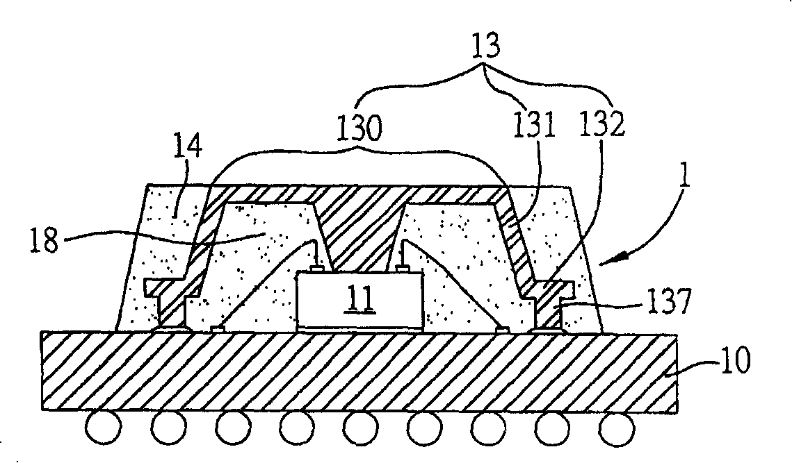
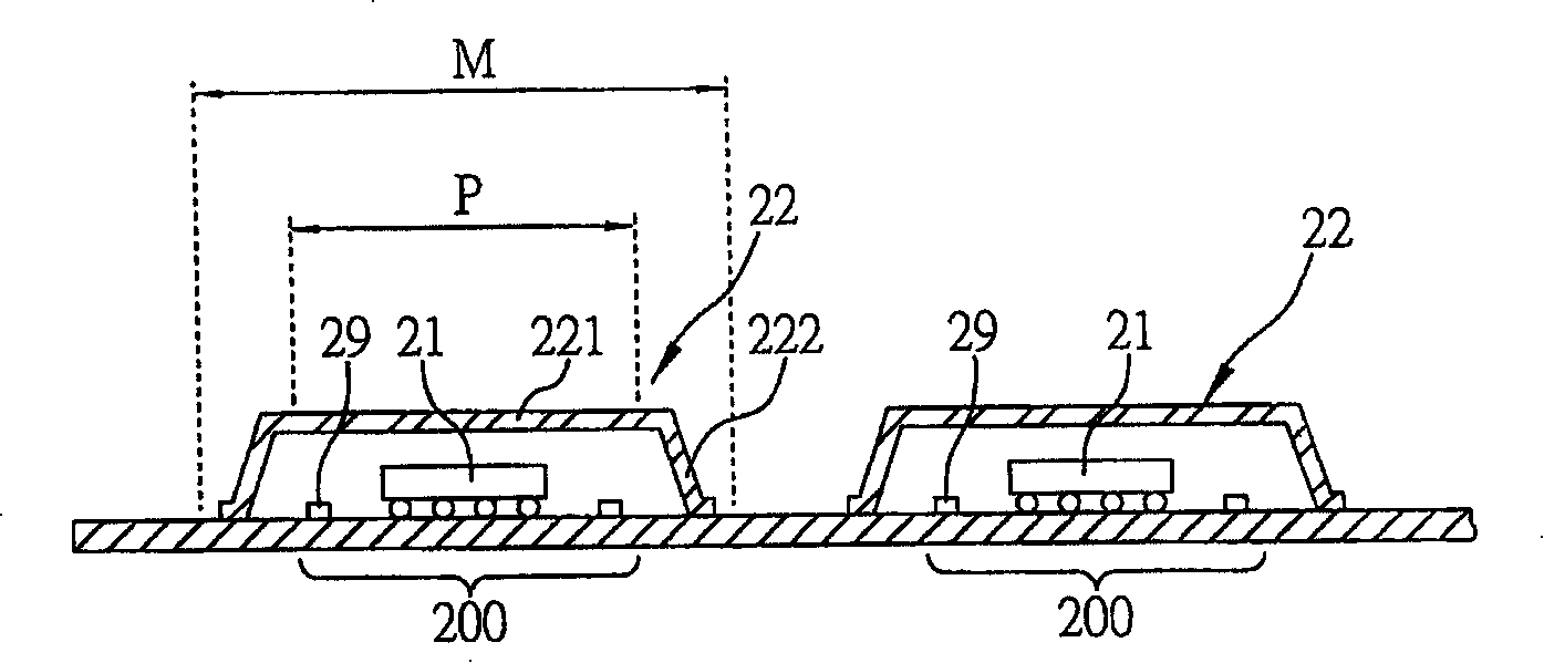
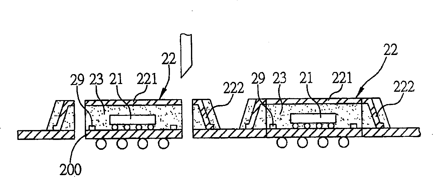
[0009] However, in the aforementioned heat-dissipating semiconductor package, because the supporting part of the heat-dissipating structure is located outside the preset plane size of the semiconductor package, that is, the supporting part is not in the semiconductor package after the cutting operation, so the heat dissipation cannot be achieved. The structure is connected and electrically connected to the substrate ground area to form a ground loop (ground), but it cannot provide shielding effect against electromagnetic interference (EMI)
[0010] In addition, although U.S. Patent No. 5,877,552 discloses that the supporting part of the heat dissipation structure can be connected and electrically connected to the substrate grounding area, but because the supporting part is directly placed in the half-body package package, the above-mentioned substrate space will be wasted. Limit the configuration of passive components
That is to say, the heat dissipation structure still has to rely on the supporting part to be connected to the substrate, so it will still cause a waste of valuable space on the substrate
[0011] Furthermore, the heat dissipation structures disclosed in the above-mentioned prior art all have to be prepared with supporting parts for the heat dissipation structures to be placed on the substrate. The cost of materials is increased, which in turn increases the cost of the process

Method used


Image

  • Cooling type semiconductor packaging member
  • Cooling type semiconductor packaging member
  • Cooling type semiconductor packaging member

Examples


no. 1 example

[0063] see Figure 3A and Figure 3B , is a plan view and a schematic cross-sectional view of the first embodiment of the heat dissipation semiconductor package of the present invention.

[0064] As shown in the figure, the heat dissipation semiconductor package includes a substrate 30, the surface of the substrate 30 is provided with a plurality of solder pads 301 and at least one ground pad 302; at least one semiconductor chip 31 is connected to the substrate 30 and electrically connected to the solder pad 301; a plurality of passive components 391 connected to and electrically connected to the substrate pad 301; at least one zero-resistance passive component 392 connected to and electrically connected to the substrate ground pad 302; and a heat sink 32, connected to the passive element 391, and electrically connected to the zero-resistance passive element 392.

[0065] The substrate 30 is, for example, a ball grid array substrate, and a plurality of solder pads 301 and at...

no. 2 example

[0075] see Figure 4A to Figure 4C , is a schematic diagram of the second embodiment of the heat dissipation semiconductor package of the present invention, wherein the Figure 4B for correspondence Figure 4A A schematic cross-sectional view of a heat-dissipating semiconductor package.

[0076] What is disclosed in the second embodiment of the heat dissipation semiconductor package of the present invention corresponds to the situation where a general passive element cannot be used as a support structure for a heat sink, or to avoid damage to it, it can be placed at the proximal corner of the substrate 30 (such as Figure 4A and Figure 4B shown) or near the edge (as Figure 4C As shown), a plurality of ground pads 302 are formed, and at least three zero-resistance passive components or metal blocks 38 are placed and electrically connected on the ground pads 302, and at the same time, solder pads 301 are provided on the rest of the substrate 30 for grounding. Place and ele...

no. 3 example

[0078] see Figure 5 , is a schematic diagram of the third embodiment of the heat dissipation semiconductor package of the present invention, the heat dissipation semiconductor package of this embodiment is substantially the same as the previous embodiment, the main difference is that the heat sink 32 can be connected to the heat sink 32 through the thermal conductive adhesive 37 at the same time on the semiconductor chip 31 to enhance the dissipation of heat generated by the semiconductor chip 31 during operation.


PUM


Abstract

The invention discloses a radiation semiconductor package, comprising a substrate which is provided with a plurality of welding pads and grounding pads on the surface, semiconductor chips which are arranged on the substrate and electrically connected with the welding pads, passive components which are arranged on the welding pads of the substrate, zero resistance passive components or metal blocks which are arranged on the grounding pads of the substrate, and radiation fins which can be arranged on the zero resistance passive components or metal blocks, wherein, the radiation fins are electrically connected with the zero resistance passive components or metal blocks, and are electrically coupled with the grounding pads of the substrate to form a ground, thereby providing an EMI blackout effect, preventing the problems of increased cost of structure process and material consumption generated when the prior heat conductive structure provided with a supporting part is arranged on the substrate through the supporting part, and preventing the problem of arrangement of electronic components on the substrate restricted by the arrangement of the supporting part.

Description

technical field [0001] The invention relates to a semiconductor package, in particular to a semiconductor package integrated with a heat dissipation structure. Background technique [0002] With the demand for thinner, lighter and smaller electronic products, the Ball Grid Array (BGA) Semiconductor Package (Ball Grid Array Semiconductor Package) can provide a sufficient number of input / output connection terminals (I / O Connection) to meet the requirements of high-density electronic products. The demand for components and semiconductor chips for electronic circuits has gradually become the mainstream of packaged products. However, since this kind of semiconductor package provides higher density electronic circuits (Electronic Circuits) and electronic components (Electronic Components), the heat generated during operation is also relatively high. If the heat on the chip surface is not quickly released in real time , The accumulated heat will seriously affect the electrical fun...

Claims


Application Information

Patent Timeline
Patent Type & Authority Applications(China)
IPC IPC(8): H01L25/00H01L25/16H01L23/367H01L23/552H01L23/488
CPCH01L23/4334H01L2224/73253H01L23/3121H01L23/552H01L2224/16225
Inventor 陈锦德杨格权葛中兴
Owner SILICONWARE PRECISION IND CO LTD
Learn More