Resistor structure and its forming method

A technology of resistors and integrated circuits, applied in the direction of electric solid-state devices, circuits, electrical components, etc., can solve the problems of proportionality and consistency of differential resistance values, uneven voltage, etc.

Active Publication Date: 2008-07-16
TAIWAN SEMICON MFG CO LTD
View PDF0 Cites 4 Cited by
  • Summary
  • Abstract
  • Description
  • Claims
  • Application Information

AI Technical Summary

Problems solved by technology

[0004] In addition, traditional resistors have relatively poor resistance-matching uniformity, which w...

Method used


Image

  • Resistor structure and its forming method
  • Resistor structure and its forming method
  • Resistor structure and its forming method

Examples


Embodiment Construction

[0026] In order to make the above and other objects, features, and advantages of the present invention more comprehensible, the preferred embodiments are specifically listed below, together with the accompanying drawings, and are described in detail as follows:

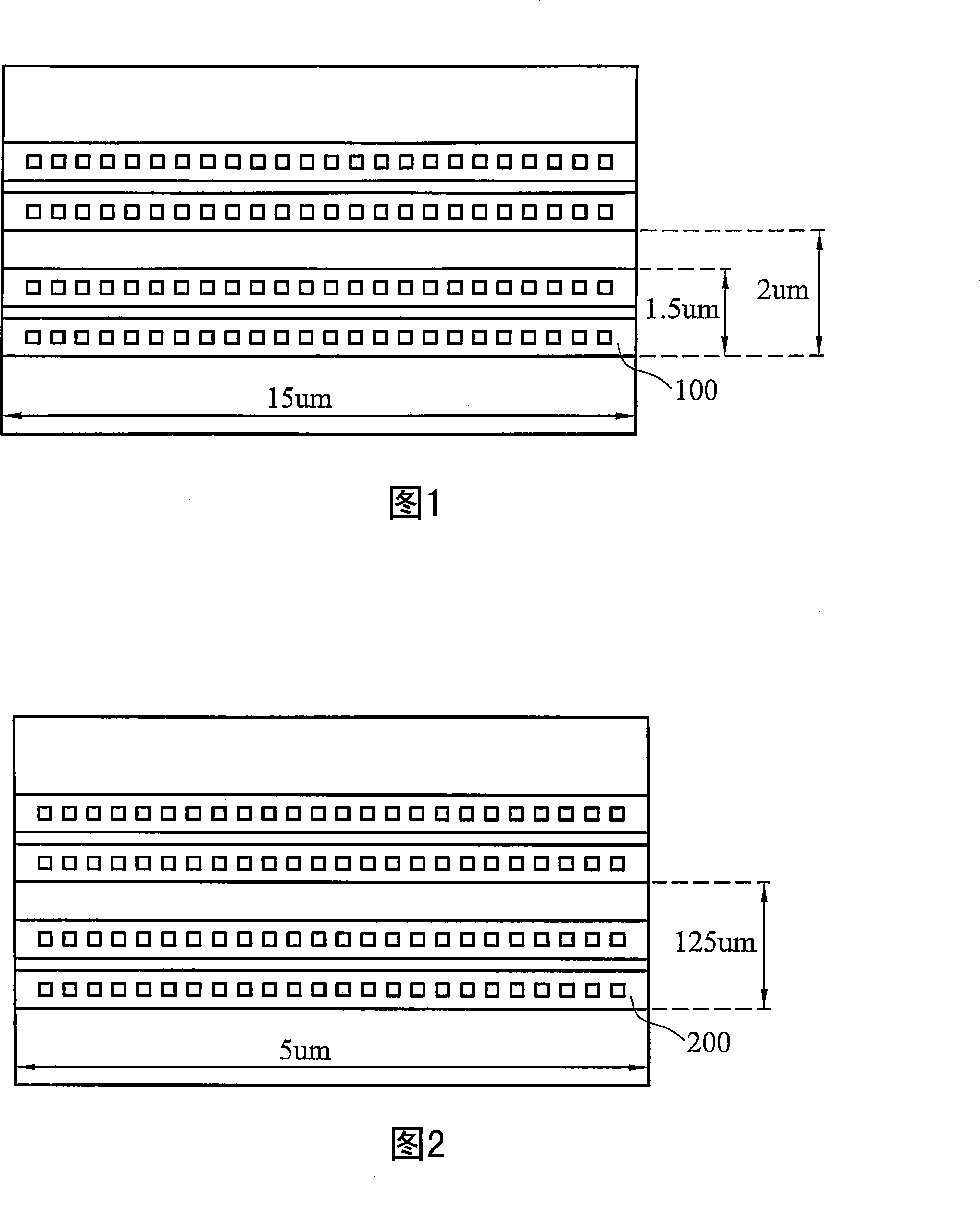
[0027] FIG. 1 shows a top view of a polycide resistor 100, which occupies a relatively large layout area. In a conventional analog-to-digital converter, a reference voltage resistor ladder circuit needs to be wide enough in physical dimension to minimize the variation in resistance value due to process variation, which allows large current flow Switching noise is thus minimized via the resistor ladder described above. The sheet resistance of the polycide layer should be about 10 ohms / sq, and the resistor 100 needs to be 15 μm wide and 1.5 μm long to provide 1 ohm resistance. Taking critical space requirements into consideration, the length of resistor 100 needs to be a minimum of 2 μm. Therefore, resistor 100 requir...


PUM

PropertyMeasurementUnit
Sizeaaaaaaaaaa
Sizeaaaaaaaaaa

Abstract

The invention discloses a resistor structure and method for forming the same. The resistor structure for an integrated circuit includes a first set of contacts connected between a semiconductor layer and a first conductive layer; a second set of plugs connected between the first conductive layer and a second conductive layer, wherein the first set of contacts and the second set of plugs are coupled together as a first resistor segment to provide a predetermined resistance for the integrated circuit; a third set of contacts connected between the semiconductor layer and the first conductive layer; a fourth set of plugs connected between the first conductive layer and the second conductive layer; wherein the contacts of the third set are coupled with the plugs of the fourth set as a second resistor segment adjacent to the first resistor; and a conductive graph serially connected to the first and the second resistors.

Description

technical field [0001] The present invention relates to integrated circuit design, and in particular to a stacked resistor structure suitable for use in integrated circuits. Background technique [0002] An integrated circuit often contains many resistors. For example, an analog-to-digital converter (ADC) may include groups of resistors to divide the voltage. Ideally, the resistance values ​​of these resistor groups should be matched to divide the voltage equally. Traditionally, the above-mentioned resistors are manufactured by forming some silicide or non-silicide polysilicon layers on a silicon wafer; the above-mentioned resistors can also be manufactured by forming N-type or P-type doped regions on the semiconductor substrate of the wafer. device. [0003] One of the disadvantages of the conventional resistors described above is that they require a large surface area. For example, for a reference voltage resistor-ladder used in an 8-bit analog-to-digital converter, th...

Claims


Application Information

Patent Timeline
IPC IPC(8): H01L27/02H01L23/522H01L29/86
CPCH01L23/5228H01L2924/0002H01L2924/00
Inventor 薛福隆林松杰
Owner TAIWAN SEMICON MFG CO LTD
Why Eureka
Try Eureka