Display device
A display device and secondary display technology, which is applied to static indicators, instruments, etc., can solve the problems of increased drive signal line power, high display pattern frequency, and insufficient power consumption, so as to ensure low power and suppress image quality deterioration , the effect of less data
- Summary
- Abstract
- Description
- Claims
- Application Information
AI Technical Summary
Problems solved by technology
Method used
Image
Examples
Embodiment 1
[0049] Embodiment 1 is to illustrate that in the partial display / less grayscale display mode, scan every 2 lines during the first half of a frame period and write the grayscale signal (such as grayscale voltage) corresponding to the display data An example in which no line is scanned in the second half of one frame period in the entire screen.
Embodiment 2
[0050] Example 2 is to illustrate that in the partial display / less gray scale display mode, scan every 2 lines in the first half of a frame period and write the gray scale signal corresponding to the display data into the first half In some areas, scan every 4 lines in the remaining 1 / 3 period of the first half of a frame period and write a low grayscale signal different from the display data, and do not scan in the second half of a frame period Example of any line.
[0051] [Example 1]
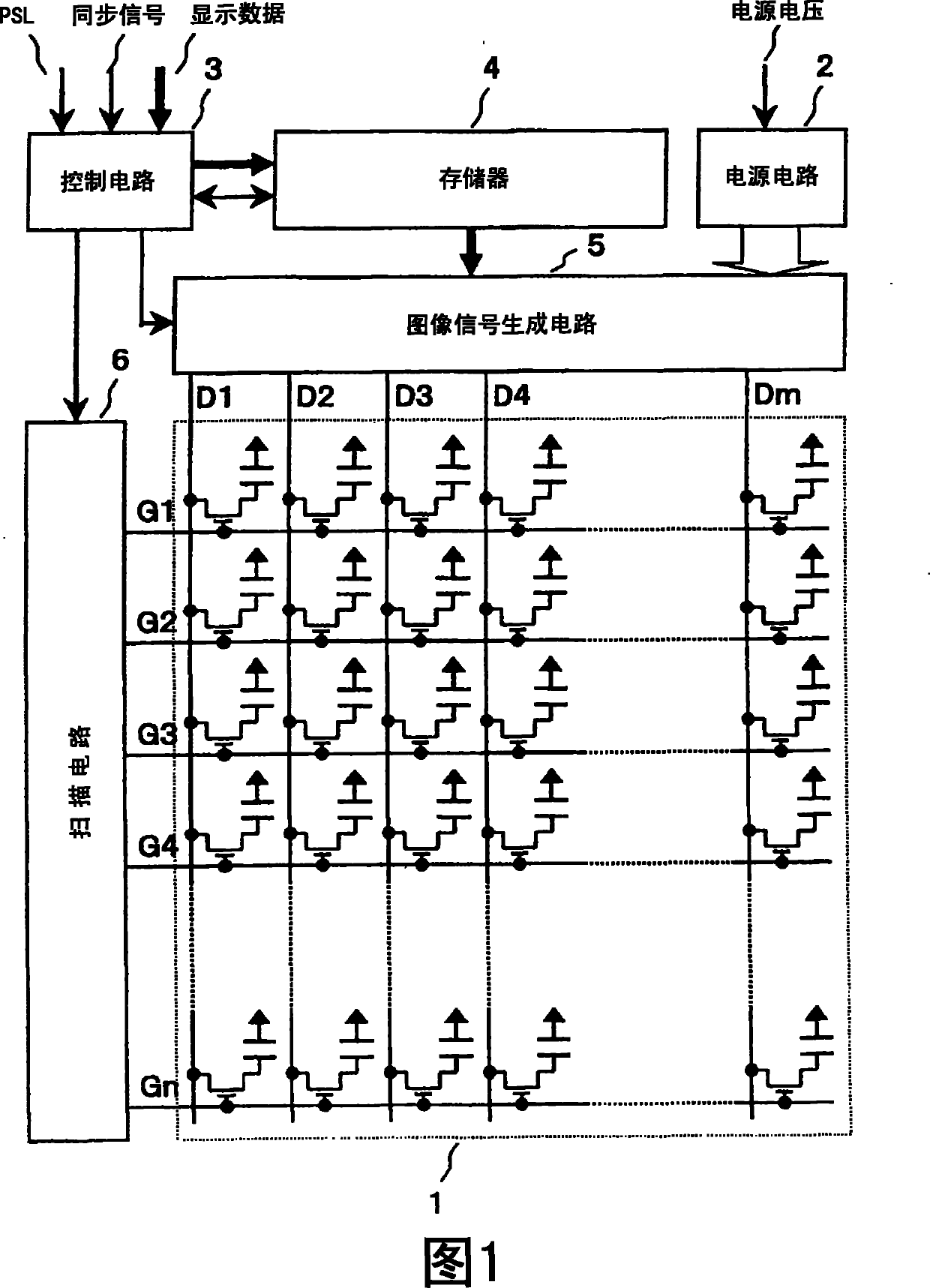
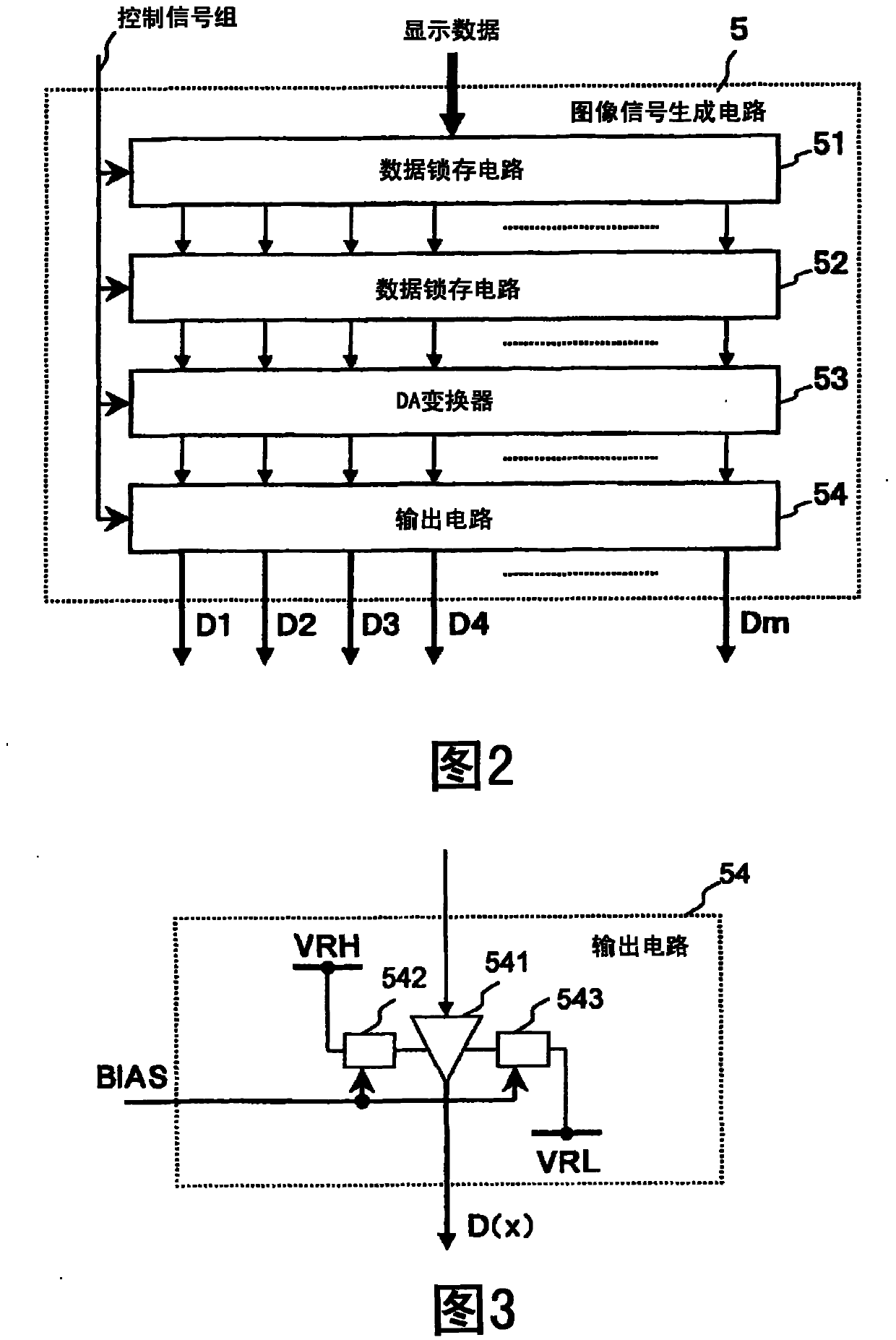
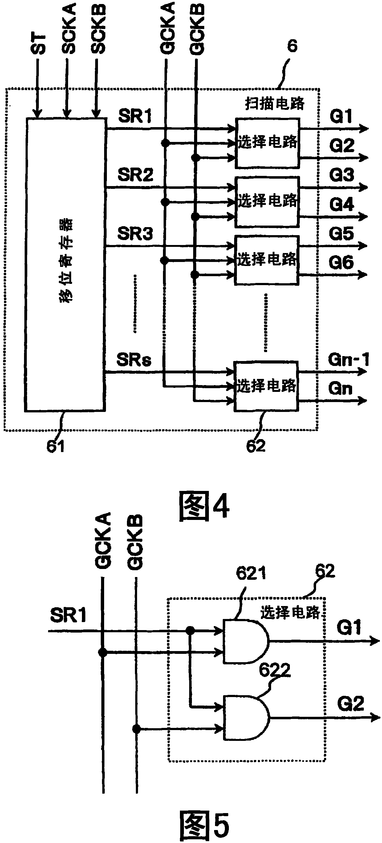
[0052] FIG. 1 is a structural diagram of a display device according to Embodiment 1 of the present invention. In Fig. 1, 1 is a display panel in which a plurality of pixels are arranged in a matrix shape; 2 is a power supply circuit for generating grayscale voltages necessary for display from a power supply voltage; 3 is input of PSL signals, Synchronous signal and other control signals or setting values and display data, control circuit for generating and outputting control signals; 4 is a...
Embodiment 3
[0097] FIG. 16 is a structural diagram of a display device of the present invention. In FIG. 16, the input signal INPUT_SIG and the control signal REG are input into the signal voltage generation circuit 11 from the outside, and the signal voltage generation circuit 11 generates and applies the signal line SIGn (n=1 to N, N is an integer) according to the input signal INPUT_SIG. signal voltage. Furthermore, the signal voltage generating circuit 11 generates an AC signal M to be supplied to the common scanning circuit 12 based on the input control signal REG.
[0098] Also, the signal voltage generating circuit 11 generates the scanning signal SFT_ST supplied to the common scanning circuit 12 and the gate scanning circuit 13 according to the synchronization signal in the input signal INPUT_SIG, and generates the high-level common voltage VCOMH and the low-level common voltage supplied to the common scanning circuit 12 . level common voltage VCOML.
[0099] The common scanning...
PUM
 Abstract
Description
Claims
Application Information


