Chip bonding machine platform and heating plate thereof

A technology of bonding machine and heating plate, which is applied in the direction of conveyor objects, electrical components, electric solid devices, etc., can solve the problems of difficulty in failure analysis work, slow speed, inconvenient rotation, etc., to avoid electrostatic damage to devices, simplify Machine structure, the effect of avoiding bending

Inactive Publication Date: 2008-07-30
SEMICON MFG INT (SHANGHAI) CORP +1
View PDF0 Cites 7 Cited by
  • Summary
  • Abstract
  • Description
  • Claims
  • Application Information

AI Technical Summary

Problems solved by technology

[0006] 1. When bonding chips or taking chips, use tweezers to clamp the devices and place them on the three card slots in turn, and the speed is relatively slow;
[0007] 2. When the specification of the device changes, it must be turned over by the heating plate before it can be used. It is very inconvenient to rotate, and the temperature of the handle 1 is high, which is easy to burn the staff;
[0008] 3. The devices waiting to be recycled must be poured out of the anti-stat

Method used


Image

  • Chip bonding machine platform and heating plate thereof
  • Chip bonding machine platform and heating plate thereof
  • Chip bonding machine platform and heating plate thereof

Examples


Example Embodiment

[0030] The chip bonding machine and its heating plate of the present invention will be described in further detail below with reference to the accompanying drawings.

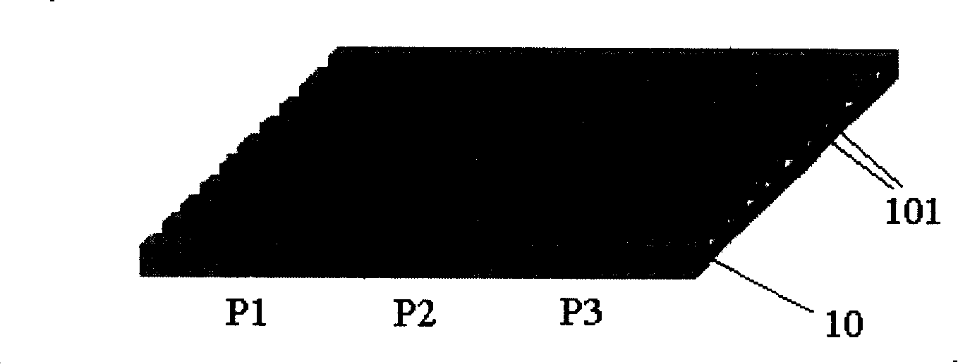
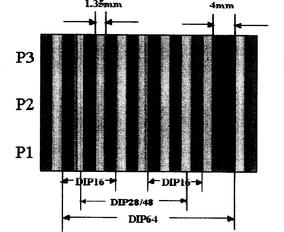
[0031] The chip bonding machine of the present invention at least includes a heating plate, a temperature control device and a vacuuming device connected to the heating plate. figure 2 It is a schematic diagram of the structure of the heating plate, which is divided into three heating areas P1, P2, P3 along the longitudinal direction, and the temperature gradually increases, and the temperature of each heating area is controlled by a temperature control device. Several parallel grooves 10 are provided on the surface of the heating plate. Each groove 10 is provided with at least one vacuum hole 101 (two are shown in the figure) corresponding to the highest temperature area P3, and each hole 101 is controlled by a vacuum device. The open and closed state.

[0032] The width of the card slot 10 on the heating plate an...


PUM


Abstract

The invention provides a chip bonder and a heater plate thereof and relates to a semiconductor test process. The heater plate of prior chip bonder can not be used for devices of different specifications unless the heater plate is rotated and turned over and is used inconveniently. The heater plate of the chip bonder is provided with three heating zones longitudinally for fixing devices and heating the devices to different extent. The device is provided with two parallel lines of pins. The surface of the heater plate is provided with a plurality of parallel card slots longitudinally; each card slot is provided with at least a hole for vacuumizing. The invention further provides a chip bonder. The heater plate provided by the invention can be used for bonding chips of devices of a plurality of specifications without rotating the heating surface of the heater plate. In addition, when the heater plate is used for devices of small specifications, a plurality of devices can be operated synchronously. The recovery efficiency of devices is improved in coordination with electrostatic-proof pipe clips to prevent the pins of the devices from bending and the devices from being damaged by static of human bodies.

Description

technical field [0001] The invention relates to a semiconductor testing process, in particular to a chip bonding machine platform. Background technique [0002] In the manufacturing process of semiconductor devices, in order to test the reliability of the process, the staff need to do a lot of experiments, among which the package level reliability (Package Level Reliability) experiment needs to use the side braze (Side braze) package form (SBA) . Chip bonding (Die Bond) is an essential step in the SBA process. It is mainly to pass the cut chip through a high temperature above 460 degrees Celsius and rub it with the gold-plated copper sheet on the shell, and then tightly bond with the copper sheet. Prepare for the next line. On the other hand, the chip bonding machine can also remove the chip from the device by heating the temperature. First, the failed sample can be used for failure analysis. Second, the tube shell can be recycled and reused to save packaging costs. . ...

Claims


Application Information

Patent Timeline
IPC IPC(8): H01L21/00H01L21/50H01L21/60H01L21/677H01L21/683
CPCH01L24/75
Inventor 卢秋明马瑾怡
Owner SEMICON MFG INT (SHANGHAI) CORP
Why Eureka
Try Eureka