Multi-chip stacking structure and its making method
A stacked structure, multi-chip technology, applied in semiconductor/solid-state device manufacturing, electrical components, electrical solid-state devices, etc., can solve the problem of increased manufacturing costs and steps, unfavorable production of thin electronic devices, and the inability to effectively reduce the height of multi-chip stacked structures, etc. problem, to achieve the effect of increasing the number of chip stacks, avoiding the increase in cost and steps
- Summary
- Abstract
- Description
- Claims
- Application Information
AI Technical Summary
Problems solved by technology
Method used
Image

Examples
no. 1 example
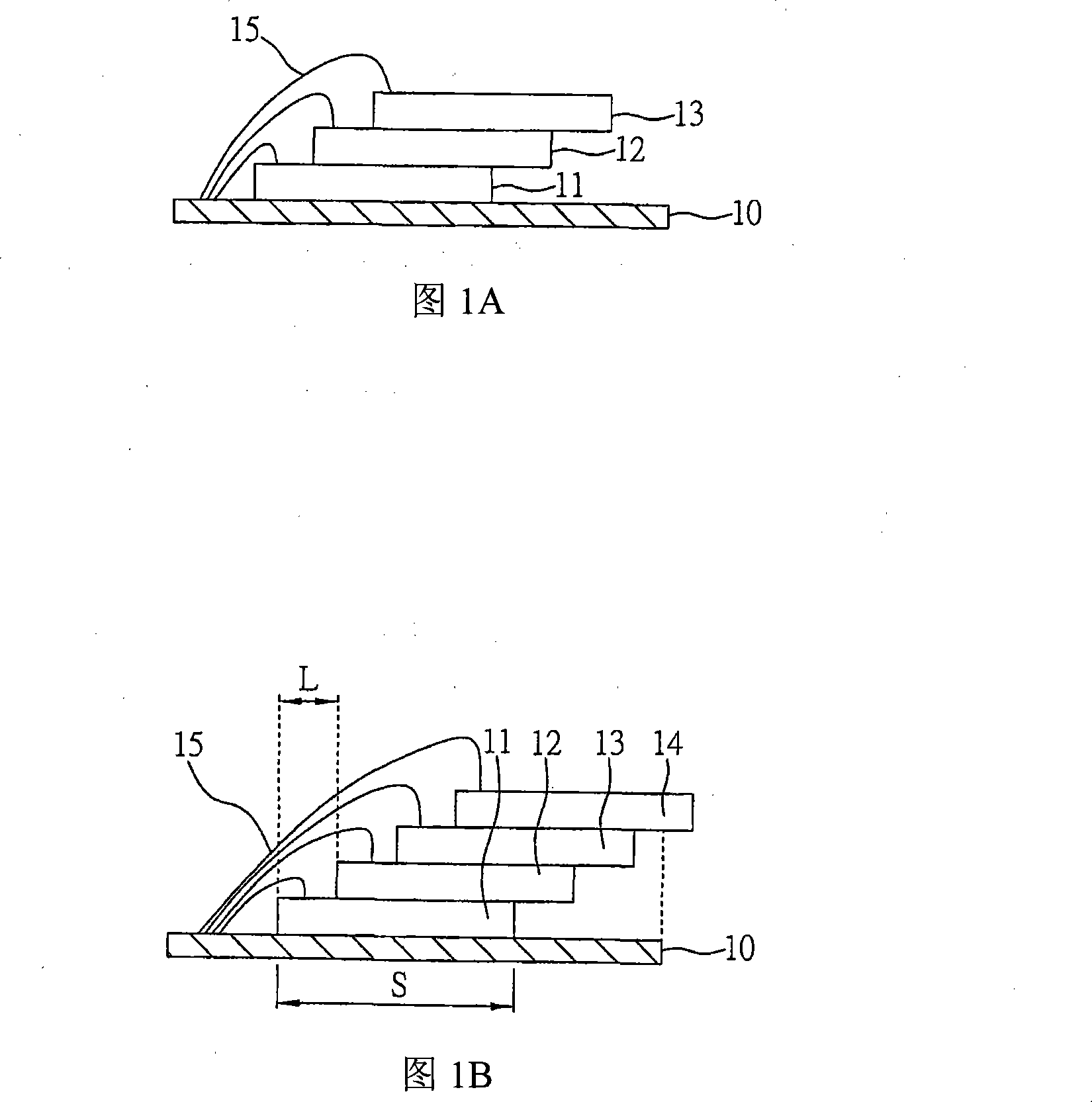
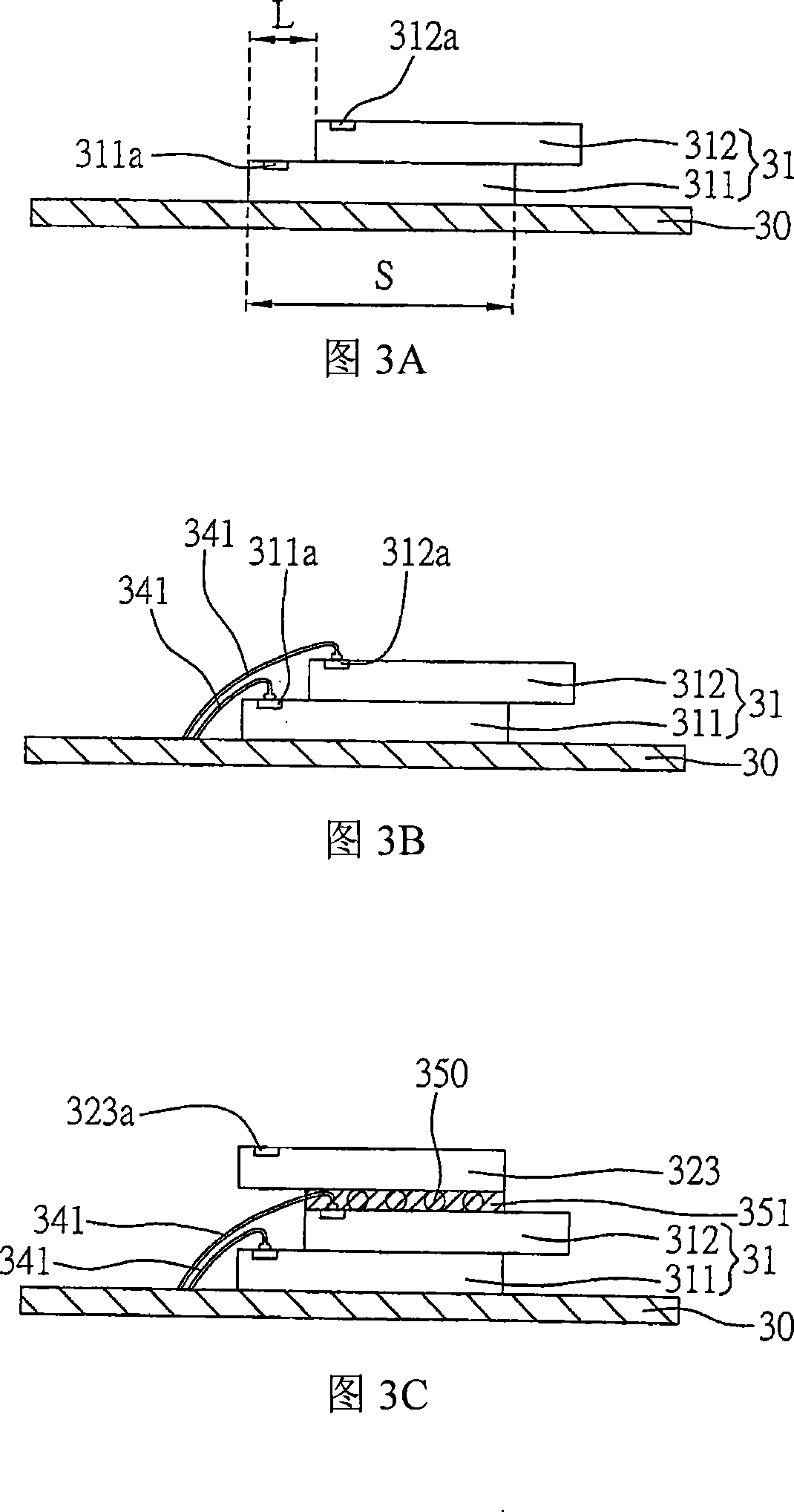
[0063] Please refer to FIG. 3A to FIG. 3F , which are schematic cross-sectional views of the first embodiment of the multi-chip stacking structure and its manufacturing method of the present invention.
[0064] As shown in Figure 3A and Figure 3B, a chip carrier 30 and a plurality of chips 311, 312 are provided, wherein the surface edges of the chips 311, 312 are provided with a plurality of welding pads 311a, 312a, so that the first chip 311 therein Adhesive on the chip carrier 30 with adhesive such as conductive adhesive or non-conductive adhesive (not shown), and then offset the second chip 312 with adhesive such as conductive adhesive or non-conductive adhesive (not shown) The lower first chip 311 is bonded on the first chip 311 in a stepwise manner at the bonding pad 311a to form the first chip group 31 . The chip carrier 30 can be a ball grid array (BGA) substrate, a land grid array (LGA) substrate or a lead frame structure.
[0065] Next, the bonding pads 311 a , 312 a...
no. 2 example
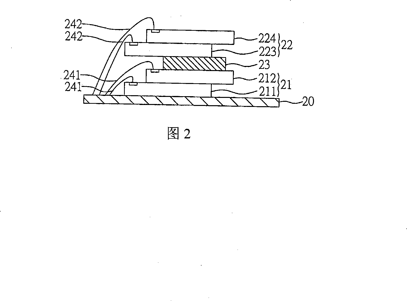
[0077] Please refer again to FIG. 4A to FIG. 4F , which are schematic diagrams of a second embodiment of the multi-chip stacking structure and its manufacturing method of the present invention. The multi-chip stacking structure and its manufacturing method of this embodiment are roughly the same as those of the foregoing embodiments, the main difference being that the bottom chip of the second chip set is connected to the second chip set using Film over Wire (FOW) technology. On the topmost chip of a chipset. In addition, to simplify the drawings and descriptions, the same or similar elements in this embodiment are represented by the same element symbols.
[0078]As shown in Figure 4A, a chip carrier 30 and a plurality of chips 311, 312 are provided, and the surface edges of the chips 311, 312 are provided with a plurality of welding pads 311a, 312a, so that the first and second chips 311, 312 Deviate from the direction of the chip pads and stack on the chip carrier 30 in a s...
no. 3 example
[0084] Please refer again to FIG. 5 , which is a schematic diagram of a third embodiment of the multi-chip stacking structure and its manufacturing method of the present invention. The multi-chip stacking structure and its manufacturing method of this embodiment are roughly the same as those of the previous embodiments, the main difference is that the top chip of the first chip set can be electrically connected to the chip carrier by reverse soldering, so as to further reduce the overall stacking structure. the height of.
[0085] As shown in the figure, the second chip 312 on the top layer of the first chip group 31 can be bonded to the pad 312a of the second chip 312 at the outer end of the bonding wire 341 by means of reverse bonding (Reverse Wire Bond). to form a stud (not shown), and then welded from the chip carrier 30, lead up and welded to the stud, so that the inner end of the welding wire 341 is stitched (Stitch Bond) to the second chip 312 In this way, the arc heig...
PUM
 Abstract
Description
Claims
Application Information
 - R&D
- Intellectual Property
- Life Sciences
- Materials
- Tech Scout
- Unparalleled Data Quality
- Higher Quality Content
- 60% Fewer Hallucinations
Browse by: Latest US Patents, China's latest patents, Technical Efficacy Thesaurus, Application Domain, Technology Topic, Popular Technical Reports.
© 2025 PatSnap. All rights reserved.Legal|Privacy policy|Modern Slavery Act Transparency Statement|Sitemap|About US| Contact US: help@patsnap.com