LDMOS transistor

A technology of transistors and semiconductors, which is applied in the manufacture of electric solid-state devices, semiconductor devices, semiconductor/solid-state devices, etc. It can solve the problems of unfavorable and reduced RF power output efficiency of LDMOS transistors, and achieve the effect of reducing the total area

Inactive Publication Date: 2008-08-06
NXP BV
View PDF1 Cites 12 Cited by
  • Summary
  • Abstract
  • Description
  • Claims
  • Application Information

AI Technical Summary

Problems solved by technology

Relatively large output capacitance can adversely reduce the RF power output efficiency of the LDMOS transistor, which is defined as the RF output power divided by the DC input power of the LDMOS transistor

Method used


Image

  • LDMOS transistor
  • LDMOS transistor
  • LDMOS transistor

Examples


Embodiment Construction

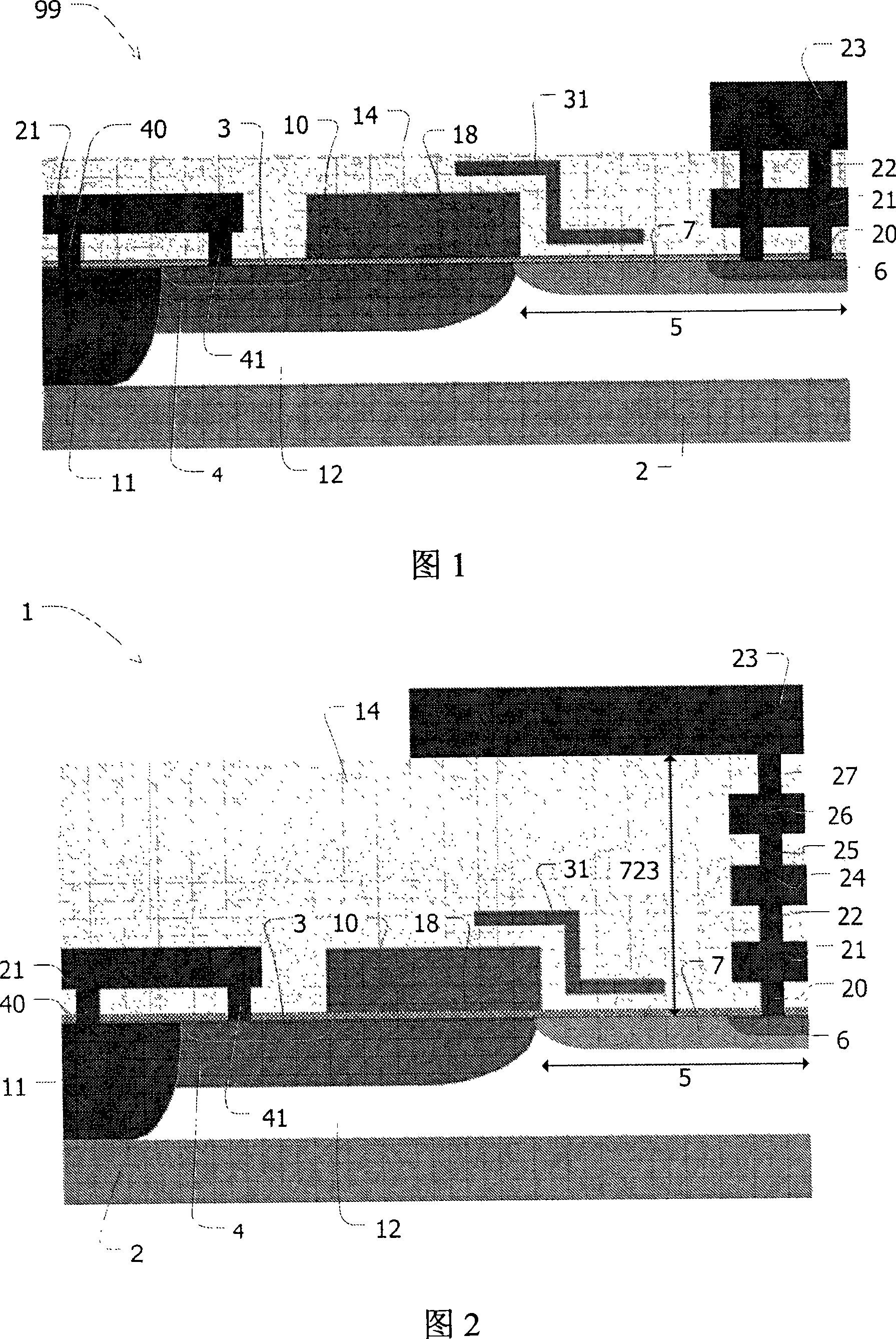
[0021] Figure 1 shows a cross-sectional view of a conventional LDMOS transistor 99 according to the prior art, comprising a substrate 2 of semiconductor material, in this case p-type silicon, on which a p-type epitaxial layer 12 is formed. The LDMOS transistor 99 also includes an n-type source region 3, an n-type drain region 5 and a polysilicon gate electrode 10, which can be equipped with a silicide layer for the polysilicon gate electrode 10 according to the situation and the polysilicon gate electrode 10 is in the channel region 4 Extending above, the polysilicon gate electrode 10 is in this example a laterally diffused p-type region. The source region 3 and the drain region 5 are connected to each other via the channel region 4 . The p-type substrate contact region 11 is electrically connected to the substrate 2 and adjoins the source region 3 on the side opposite to the side adjoining the channel region 4 . The channel region 4 , the substrate contact region 11 , the so...


PUM


Abstract

The LDMOS transistor (1) of the present invention comprises a substrate (2), a gate electrode (10), a substrate contact region (11), a source region (3), a channel region (4) and a drain region (5 ), the drain region (5) includes a drain contact region (6) and a drain extension region (7). The drain contact region (6) is electrically connected to the top metal layer (23) extending over the drain extension region (7), wherein the distance between the top metal layer (23) and the drain extension region (7) (723 ) greater than 2 μm. This reduces the area of ​​the drain contact region (6) and increases the RF power output efficiency of the LDMOS transistor (1). In another embodiment, the source region (3) is electrically connected to the substrate contact region (11) via the silicide layer (32) instead of the first metal layer (21), thereby reducing the source region ( 3) Capacitive coupling to the drain region (5) and thereby further increasing the RF power output efficiency of the LDMOS transistor (1).

Description

technical field [0001] The present invention relates to LDMOS transistors. Background technique [0002] In base stations for personal communication systems (GSM, EDGE, WCDMA), RF power amplifiers are key components. For these power amplifiers, RF laterally diffused metal-oxide-semiconductor (commonly abbreviated as LDMOS) transistors are now the technology of choice because of their exceptionally high power, gain, and linearity. In order to be able to meet the requirements imposed by new communication standards, the performance of LDMOS transistors is undergoing continuous improvement while the size continues to shrink. [0003] In WO2005 / 022645, an LDMOS transistor is disclosed which comprises source and drain regions in a semiconductor substrate in which the source and drain regions are connected to each other by a channel region . The source region and the substrate are electrically connected through the first metal layer. The LDMOS transistor also includes a gate el...

Claims


Application Information

Patent Timeline
Patent Type & Authority Applications(China)
IPC IPC(8): H01L29/78H01L29/417H01L29/45H01L29/40H01L23/482H01L23/532
CPCH01L21/76895H01L23/4827H01L23/53219H01L29/402H01L29/41725H01L29/4175H01L29/41758H01L29/456H01L29/7835H01L2924/0002H01L2924/00H01L29/66704H01L29/7816
Inventor 斯蒂芬·J·C·H·特厄乌文弗雷尔克·范瑞哲彼得拉·C·A·哈梅斯
Owner NXP BV
Why Eureka
Try Eureka