

Method for producing tiny soldered balls with repeatedly-usable substrates
A substrate and solder ball technology, applied in the field of preparing tiny solder balls, can solve the problems of easy introduction of various impurities, poor process controllability, ineffective control of droplet size and continuous growth, etc., to avoid surface oxidation, wire drawing or fluffing Phenomenon, reduce production cost, avoid fragmentation burr and adhesion effect
- Summary
- Abstract
- Description
- Claims
- Application Information
AI Technical Summary
Problems solved by technology
Method used
Image

Examples
Embodiment Construction
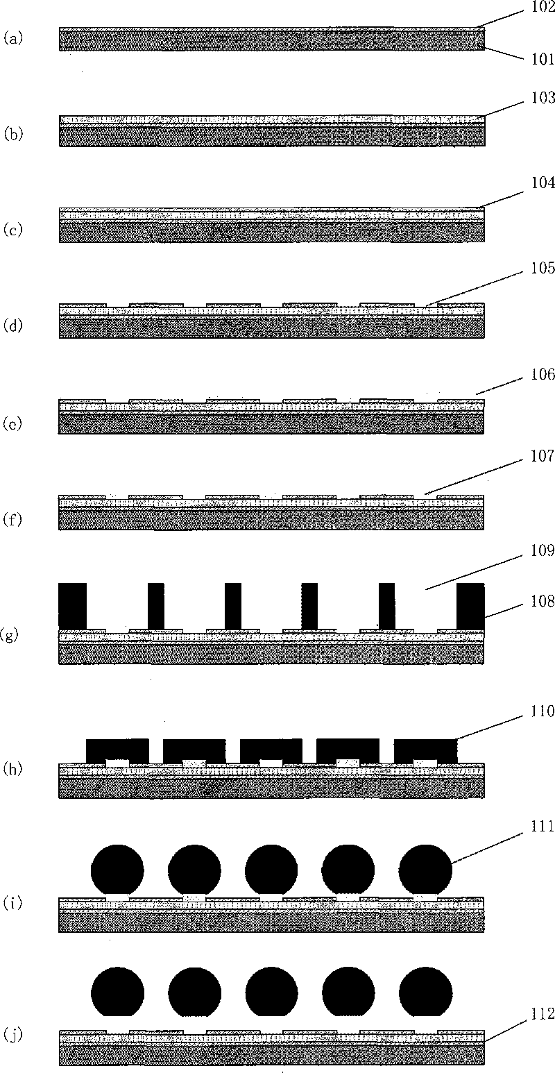
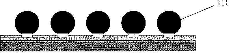
[0025] A typical micro-solder ball preparation process includes the following steps:
[0026] 1. Using IC manufacturing process to prepare reusable substrates
[0027] (1) First, the single-sided polished N-type (100) silicon wafer is cleaned, and then thermally oxidized, and the thickness of the silicon dioxide oxide layer 102 is about 0.3 microns;
[0028] (2) Vacuum sputtering metal conductive layer TiW and Au 103, the thickness is about 0.05 micron and 0.2 micron respectively; the adhesion between the silicon dioxide layer and Au is poor, so TiW is used as the metal adhesion layer on the silicon dioxide , the three layers of metals are sputtered sequentially in the same vacuum chamber;
[0029] (3) Then deposit a barrier layer SiO on the conductive layer by plasma enhanced chemical vapor deposition (PECVD) 2 or Si 3 o 4 104 with a thickness of about 0.1 micron; a circular barrier opening is photoetched to expose the conductive layer metal by using positive photoresist,...
PUM
| Property | Measurement | Unit |
|---|---|---|
| thickness | aaaaa | aaaaa |
| thickness | aaaaa | aaaaa |
| thickness | aaaaa | aaaaa |
Abstract
Description
Claims
Application Information