Eureka AIR delivers breakthrough ideas for toughest innovation challenges, trusted by R&D personnel around the world.

Method and structure for forming slot via bitline for MRAM devices

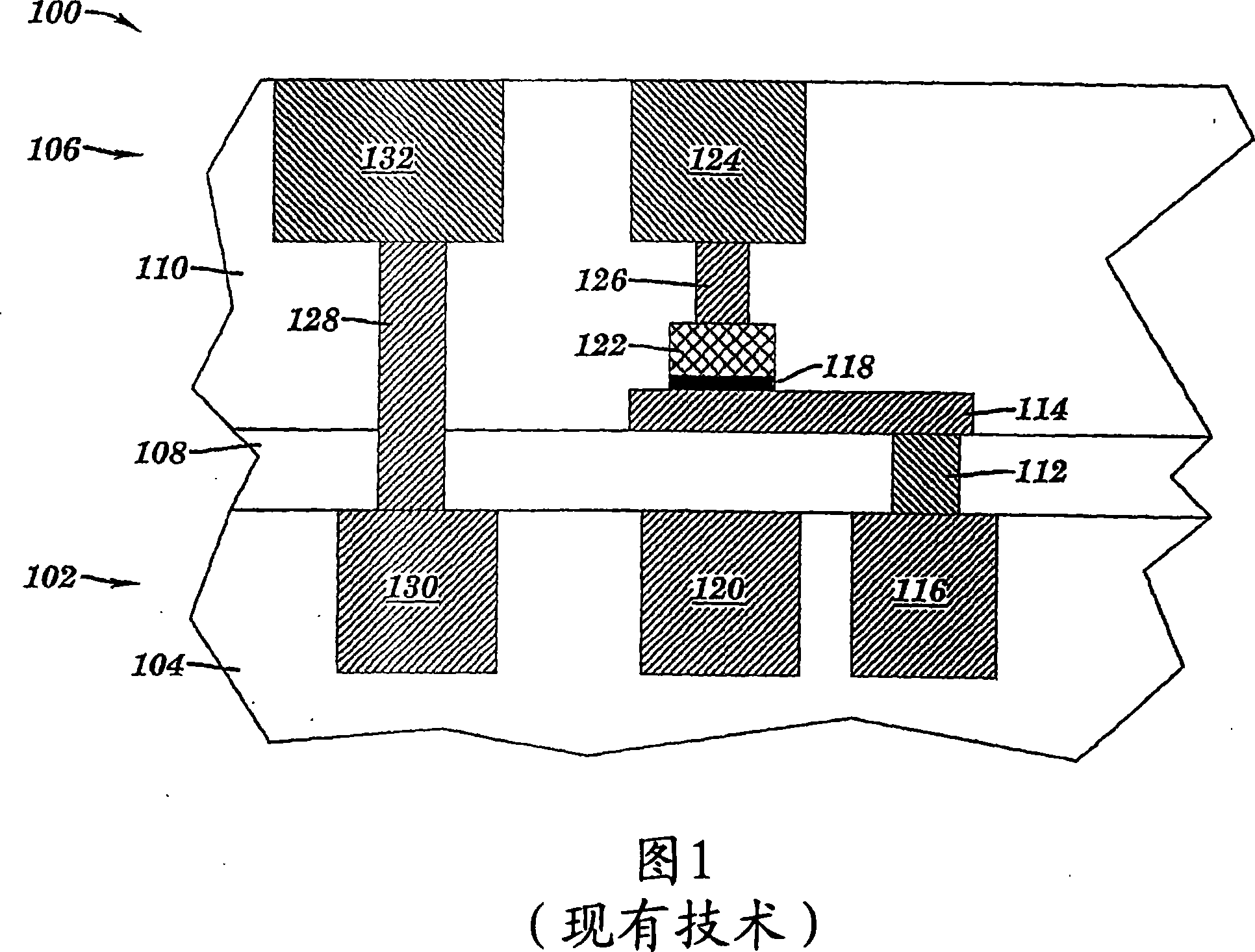
A technology of vias and devices, which is applied in the field of magnetic random access memory devices, can solve problems such as bad problems, difficult scaling of MRAM devices, and current-carrying limitations.

Inactive Publication Date: 2008-08-20
IBM CORP
View PDF0 Cites 5 Cited by
  • Summary
  • Abstract
  • Description
  • Claims
  • Application Information

AI Technical Summary

Problems solved by technology

[0007] Scaling of MRAM devices has become very difficult due to the trend towards reduced device ground rules and smaller wiring sizes, due to the current-carrying limitations of the very narrow lines used to switch the states of the MRAM cells
Ferromagnetic liners surrounding switching lines have been used to concentrate the switching field at the MTJ, however they are not expected to be as effective as line size reduction
Scaling to lower operating voltages makes the problem worse because lower impedance lines are required to pass the same amount of current

Method used


Image

  • Method and structure for forming slot via bitline for MRAM devices
  • Method and structure for forming slot via bitline for MRAM devices
  • Method and structure for forming slot via bitline for MRAM devices

Examples


Embodiment Construction

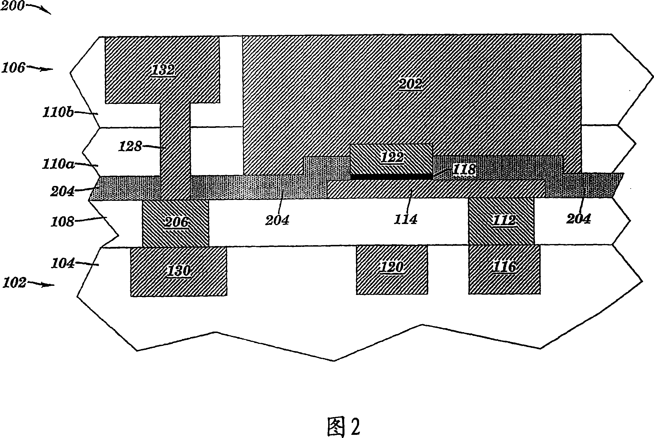
[0018] Described here is a method and structure for providing a practical means of realizing MRAM structures with greater current carrying capability in the bit lines and eliminating the need for additional masking layers to achieve this as in conventional devices . Although the structures and methods described here are presented in the context of FET-based devices, it is contemplated that the principal features of the invention are equally applicable to other structures including, but not limited to, cross-point MRAM devices, for example.

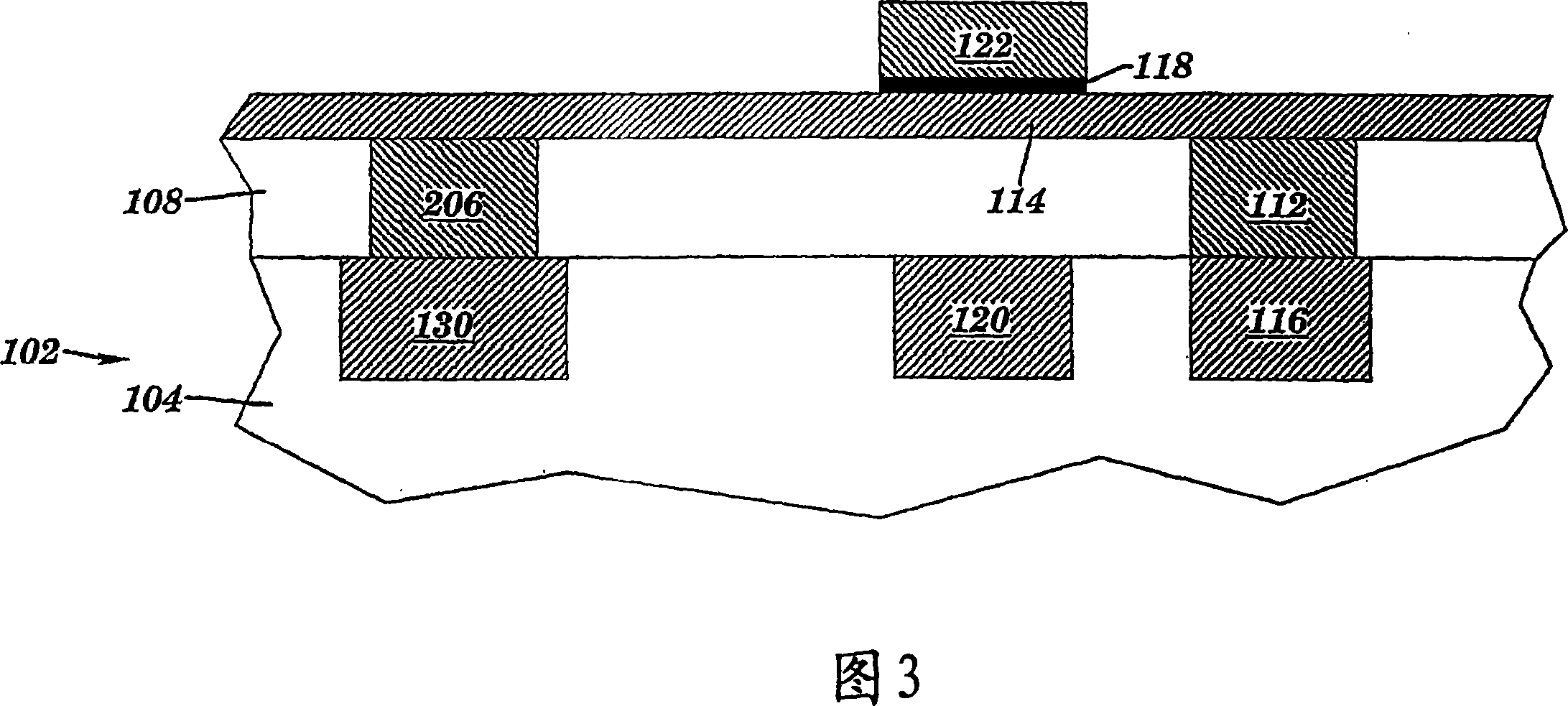
[0019] Briefly, the slotted via bitline structure was created to replace the traditional bitline and hardmask via structure, where the traditional hardmask via structure is used to place the hardmask above the magnetic stack layer is connected to the upper bit line. This can be achieved, for example, by creating an etch stop layer above the MTJ and a lateral strap connecting the bottom of the MTJ stack to the underlying wiring layer. In ...


PUM


Abstract

A magnetic random access memory (MRAM) device includes a magnetic tunnel junction (MTJ) stack formed over a lower wiring layer, a hard mask formed over the MTJ stack, and an upper wiring layer formed over the hard mask . The upper wiring layer includes a slot via bit line formed therein in contact with the hard mask and with an etch stop layer partially surrounding a sidewall of the hard mask.

Description

technical field [0001] The present invention relates generally to Magnetic Random Access Memory (MRAM) devices, and more particularly to methods and structures for forming slot via bitlines for MRAM devices. Background technique [0002] Magnetic (or magnetoresistive) random access memory (MRAM) is a non-volatile random access memory technology that can replace dynamic random access memory (DRAM) as the standard memory for computing devices. Using MRAM as non-volatile RAM enables an "instant on" system that is ready to use when turned on, thus saving traditional PCs from, for example, booting data from the hard drive during system power-on. The amount of time it takes for the drive to transfer to volatile DRAM. [0003] A magnetic memory element (also known as a tunneling magnetoresistive or TMR device) comprises a structure having ferromagnetic layers separated by insulating nonmagnetic layers (barriers) and arranged as a magnetic tunnel junction (MTJ). Digital informatio...

Claims


Application Information

Patent Timeline
Patent Type & Authority Applications(China)
IPC IPC(8): H01L29/76H01L29/94H01L31/062H01L31/113H01L31/119H10N50/01H10N50/10
CPCB82Y10/00H10B61/00H10N50/01
Inventor 迈克尔·C.·加迪斯卡尔·莱登斯劳伦斯·A.·克莱温格蒂莫西·J.·达尔顿许履尘黄洸汉杨智超
Owner IBM CORP
Why Eureka
Eureka Blog
Learn More