

Scribing method for brittlement substrate web with precision laser and special-purpose equipment
A special equipment and base material technology, which is applied in the field of precision laser scribing of brittle base materials and special equipment, can solve the problems of difficulty in ensuring the coincidence accuracy of scribe lines on the upper and lower sides, and low efficiency, so as to improve cost performance, competitiveness, and guarantee Machining accuracy, machining efficiency, and the effect of reducing precision requirements
- Summary
- Abstract
- Description
- Claims
- Application Information
AI Technical Summary
Problems solved by technology
Method used
Image

Examples
Embodiment Construction
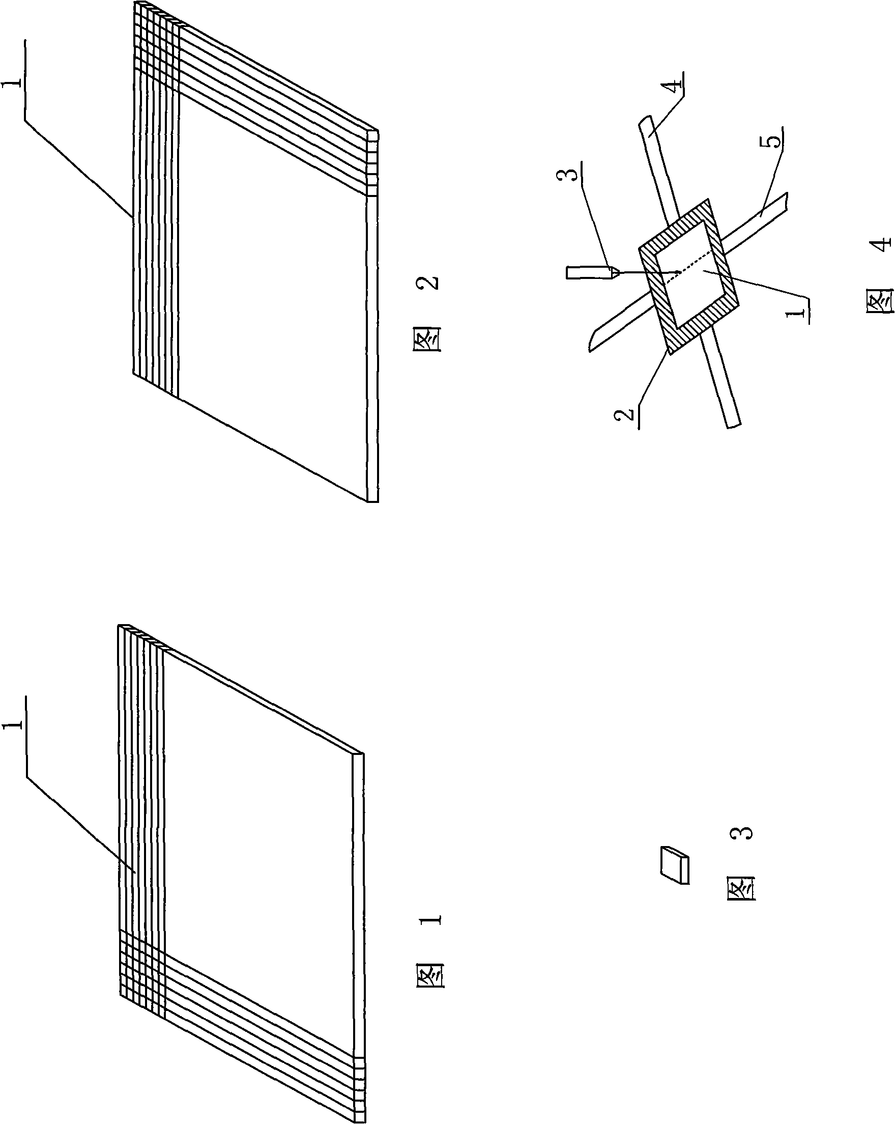
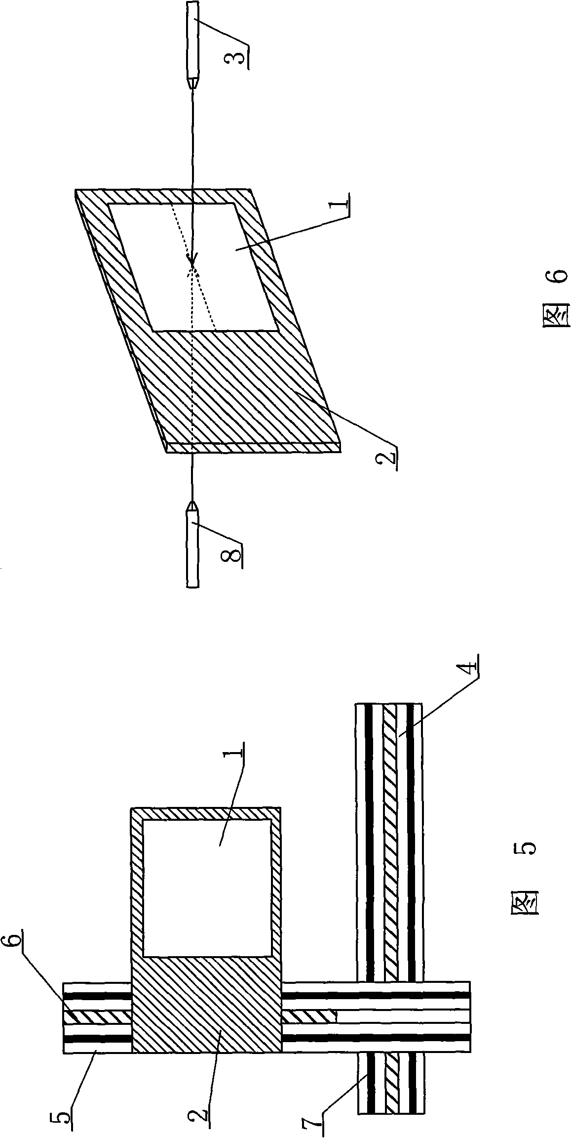
[0017] See Fig. 5 and Fig. 6, the special equipment for precision laser scribing micro-parts, which includes an X-axis-Y-axis moving table and at least one pair of laser heads 3,8. The X-axis 4 and Y-axis 5 of the mobile worktable are arranged in the vertical plane; the Y-axis 5 of the mobile worktable is embedded in the slide rail 7 of the X-axis 4 and connected with the X-axis 4 with threads, and the chuck for clamping the base material 2 and the Y-axis 5 are threadedly connected, and the chuck frame of the chuck 2 clamping the base material is arranged in a vertical plane. The processing process of the present invention is described below in conjunction with accompanying drawing: base material 1 is installed in the mouth frame of chuck 2, and base material 1 is arranged vertically, and when marking the line horizontally on base material 1 surface, laser head 3,8 After alignment, the X-axis 4 drives the Y-axis 5 to move in the horizontal direction, and the laser heads 3 and ...
PUM
 Abstract
Description
Claims
Application Information